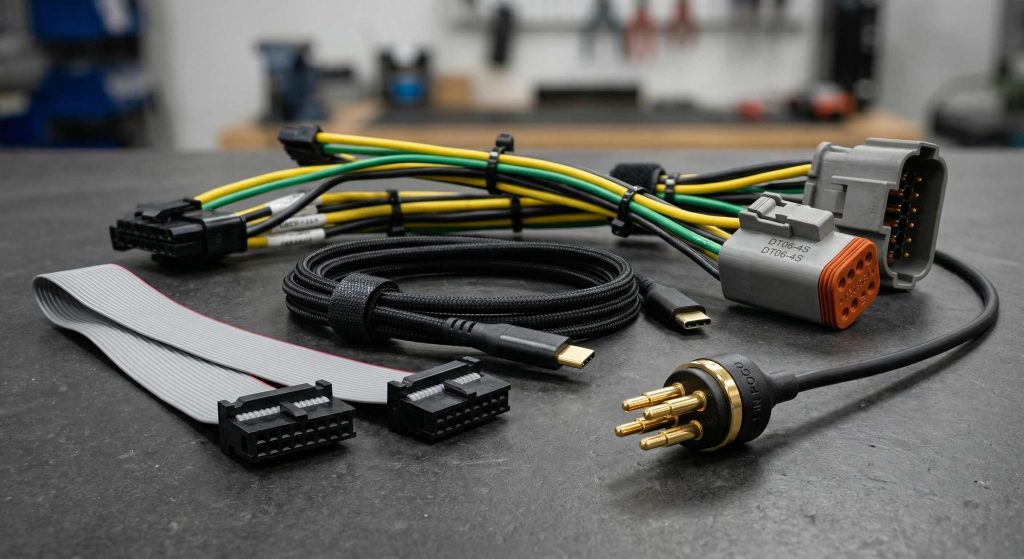
Gold Finger PCB Price: Hard Gold, ENIG and Selective Plating
A gold finger board is a connector and a circuit board at the same time, and that dual role is what makes its price different from an ordinary PCB. The fingers must survive insertion cycles, stay flat enough to mate reliably and keep contact resistance stable for years, so plating thickness and geometry matter as much as layout. This guide breaks down a gold finger PCB price into plating, layer count, beveling, inspection and tooling in 2025.
What Makes a Gold Finger Board Different
A gold finger board uses exposed plated pads along one or more board edges to mate directly with a card-edge connector, so the board becomes the plug. That removes the cost of a separate connector and the height it would occupy, which is why the format survives in expansion cards, memory modules, communication modules and industrial backplanes.
The trade is mechanical. Contact surfaces are exposed to repeated insertion and to whatever environment the product sees, so the plating must resist wear and oxidation. The pad design standards that apply to a normal soldered pad are not sufficient here, because a finger is a sliding contact rather than a fixed joint.
Plating Options and Their Cost
Hard gold plating uses a gold-cobalt or gold-nickel alloy over a nickel barrier, and it is the standard choice when the board will be inserted many times. It is specified by thickness, commonly 30 microinches for a card that is removed occasionally and 50 microinches or more for one that is cycled frequently. Thicker plating costs proportionally more because gold is the dominant material cost.
An ENIG finish is the cheaper alternative and gives a very flat surface, which suits fine-pitch fingers and boards with many fingers per edge. Its durability is lower, so it belongs on products that are inserted once or a few times. Selective gold plating covers only the fingers and leaves the rest of the board on HASL or ENIG, and it usually saves a quarter to a third of the plating cost on a large board.
Layer Count, Finger Count and Board Area
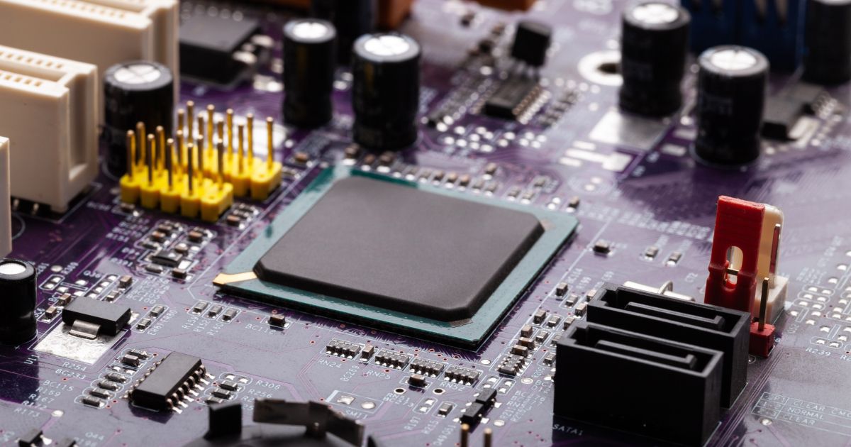
Layer count sets the fabrication base, and the finger count sets the plating and inspection load. A 2-layer board with ten fingers per edge is the entry point; a 4-layer board with twenty fingers on a controlled-impedance interface is a normal mid-range product; a 6-layer or HDI board with a dense finger field is the top of the range. Each step adds lamination, imaging and test time.
Board area interacts with plating in a way that surprises buyers. The plating charge tracks the plated area, so a long edge with wide fingers consumes more gold than a compact one, and the bevel has to be applied along the full mating edge. Reducing finger length to the functional minimum and keeping the array compact is the most direct cost saving available.
Bevel, Chamfer and Mechanical Requirements
Nickel thickness matters as much as gold thickness. The nickel barrier underneath the gold provides the hardness that resists wear and stops copper from diffusing into the gold layer, so a thin or porous nickel layer fails long before the gold does. Most specifications call for 100 to 200 microinches of nickel, and that number belongs in the purchase specification rather than being left to the plating line.
Insertion needs a lead-in. A bevel or chamfer along the mating edge guides the board into the connector and prevents the corner from catching on the contact spring. It is a separate mechanical operation, usually billed per edge, and it becomes more expensive when the edge is long, when the bevel angle is tight, or when the board is thin and needs extra support during the cut.
The mechanical side does not stop at the bevel. Fingers must be clear of the connector housing, so board outline and mounting design has to account for insertion depth, keying slots and any retention hardware. Keying must be cut before plating, because a slot cut after plating exposes bare laminate along the edge.
Design Rules That Affect Price
Finger geometry is the main design lever. Width and pitch should follow the connector the board will mate with rather than a convenient round number, and the spacing between fingers should respect the applicable insulation standard. Fingers that are longer than needed, or spaced more tightly than the connector requires, add plating cost without improving anything.
The rest of the board should follow ordinary fabrication rules so the finger area does not force a special process. Copper-to-edge clearance, solder mask dam width and minimum annular ring all have to be met on the panel that carries the fingers, so applying manufacturable design guidelines from the start keeps the board on a standard flow.
Regional Pricing and Supplier Selection
Boards with heavy gold plating are less sensitive to regional labour cost than bare FR-4 boards, because the material dominates the price. That narrows the gap between regions, but it also means a supplier who plates to a lower thickness will look cheaper for reasons that have nothing to do with efficiency. Thickness and coverage must be compared explicitly.
Selection should be based on measurable items rather than on the headline rate. Plating thickness tolerance, the ability to run selective plating, inspection method, edge quality after beveling and the willingness to supply a certificate for the plating are all worth more than a few cents of unit price.
Hidden Cost Items
Inspection is the last variable. A board with selective plating needs a step that confirms the fingers were plated and the rest of the board was not, and thick hard gold is normally verified by X-ray fluorescence rather than by cross-sectioning. Asking how plating thickness is checked, and whether a report is issued per lot, separates a supplier who controls the process from one who simply plates by time.
Tooling and setup are the largest hidden items. A plating programme, a fixture for selective plating, a bevel programme and a test fixture are each billed once, and on a small order their amortised effect is significant. Electrical test and automated optical inspection are sometimes quoted separately, especially when the finger count is high.
Shipping and duty matter as well, because gold-containing boards have a higher declared value than ordinary boards of the same size. There is also the cost of a change: moving a finger, changing a keying slot or adjusting plating thickness after tooling is ordered means new programmes. Freezing the connector interface early is the cheapest decision available.
Reducing Cost Without Losing Insertion Life
The most effective savings are geometric and selective. Use ENIG where insertion cycles are low, specify hard gold only on the fingers that need it, shorten fingers to the required contact length and keep the array on a single edge where the connector allows it. Each of those changes reduces the plated area, which is what the gold charge follows.
What should not be reduced is plating thickness on a cycled interface, bevel quality or inspection coverage. Under-plating a hard gold finger produces a board that works on the bench and fails after a few hundred insertions, and the warranty cost of that failure is far larger than the plating that was saved.
FAQ
How thick should hard gold be? Thirty microinches over nickel is a reasonable baseline for a board that is inserted occasionally, and fifty microinches or more is appropriate when the board is cycled regularly. The connector datasheet usually states the expected cycle count and the plating it needs.
Do the fingers really need a bevel? Yes, if the board is inserted by hand or by a mechanism that may misalign it. The bevel spreads the insertion force and protects both the finger and the connector spring. Removing it saves a small operation and risks damage to both parts.
Is selective plating worth it on a small board? It becomes worthwhile when the total board area is large and the finger area is a small fraction of it, because the plating charge tracks the plated area. On a small board with fingers on both edges the saving is usually too small to justify the extra programme.