Practical Notes on Audio Amplifier PCBA
An audio amplifier PCBA is a board where the measurements look simple and the listening experience is unforgiving. A switching amplifier can post excellent distortion figures and still hum audibly, because the hum comes from a ground loop or from a supply coupling that a distortion measurement at one frequency does not detect. Designing the board is therefore a matter of understanding the current paths rather than of choosing components.
This article covers what appears on an amplifier board, how the grounding should be arranged, and the thermal and noise measures that decide whether the result is quiet.
What Is on an Amplifier Board
The signal chain runs from the input connector through a buffer, a volume control and a gain stage to the power stage. Around it sit the power supply, the protection circuits and the control interface. In a device with multiple channels the same chain is repeated, and the channels share the supply and the ground.
The power stage dominates the board area and the thermal design. Whether it is a linear output stage or a switching one, it draws the largest current, produces the most heat, and is the source of the noise that the input stage has to reject. Separating those two functions physically is the first principle of amplifier layout.
Grounding and the Star Point
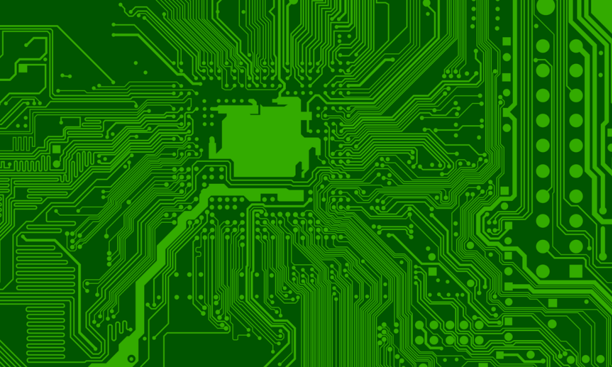
The classic approach is a star ground, in which every circuit block has its own ground return routed to a single point rather than to a shared plane. That prevents the large currents returning from the power stage from developing a voltage across the ground impedance that the input stage then measures.
On a modern board the star is usually implemented as a layout discipline rather than as a literal single point. The input section, the gain stage and the power stage each have their own ground area, and those areas are joined at one place near the supply. The important property is that no conductor is shared between the signal return and the power return, because any shared impedance converts the output current into a voltage in the input circuit. The mixed-signal layout principles apply directly to that separation.
Hum Loops and Input Wiring
Hum in an audio system is usually caused by a hum loop rather than by a single coupling path. When two grounded pieces of equipment are connected by an audio cable, the two ground connections and the cable shield form a loop, and any magnetic field passing through it induces a current that appears as hum.
The board can help by keeping the input ground separate from the chassis ground, so that the signal reference is defined by the source rather than by the chassis. Where the input is balanced, the common-mode rejection of the input stage removes most of the loop current, and the layout should preserve the balance by routing the two conductors with the same impedance to ground. A balanced input has to remain balanced all the way to the differential stage, because any asymmetry converts part of the hum into a differential signal.
Power Supply Rejection
The amplifier’s ability to ignore its supply depends on the circuit and, at high frequency, on the layout. A feedback loop that is referenced to the supply rather than to the signal ground will modulate the output as the supply moves, and the modulation appears as noise that no amount of supply filtering removes.
The layout contributes through the impedance of the supply distribution. If the output stage and the input stage share a supply trace, the current in that trace develops a voltage that reaches the input stage. Separate decoupling for each stage, placed close to the stage it serves, and a supply distribution that runs from the reservoir to the power stage without passing the input section are the practical measures. The trace width and current calculation gives the geometry, and the supply traces to the output stage should be sized for the peak current rather than the average.
Thermal Design of the Output Stage
The output devices dissipate significant power, and their junction temperature has to stay below the limit under the worst combination of signal and ambient. On a board-mounted design the copper is the heatsink, and the thermal path runs from the device through the pad and the vias into the copper areas.
The area required depends on the power and the allowed rise, and it is usually the constraint that sets the board size. Where the enclosure is sealed, the heat has to reach the case through the board or through a thermal interface, and the layout should place the output devices along the edge that contacts the heatsink. Thermal vias under a surface-mounted device, in an array with a pitch small enough to spread the heat evenly, are the standard arrangement.
Noise and Shielding
An amplifier board contains small signals and large currents, so shielding and separation are used together. The input connector and the first stage should be as far from the output stage and the supply as the board allows, and where they must be close, a grounded copper area between them reduces the coupling.
Class-D output stages deserve particular attention, because their output is a high-frequency square wave. The output filter should be placed close to the switching devices, the output trace should be routed as a tight pair to minimise the loop area, and the switching loop between the devices and their decoupling capacitors should be as small as the layout permits. Those three measures do more for the noise performance than any additional filtering.
Protection and Control
Protection circuits are part of the design rather than an addition. Over-current protection, thermal shutdown, DC offset detection and speaker protection all involve sensing circuits that must be accurate and must not introduce their own noise into the signal path.
The control interface, if there is one, brings a microcontroller and often a display onto the same board. The microcontroller should be placed away from the analogue section, its clock should be kept short, and its ground should return through the digital area rather than through the signal ground. Where the device has a standby mode, the supply arrangement has to allow the power stage to be isolated completely while the control section remains alive. The routing of the supply and its return then follows the same discipline as any high-current board, and the ground routing and power trace planning rules describe how the distribution should be arranged.
FAQ
Why does my amplifier hum even with no input connected? An open input can pick up noise, but if the hum persists with the input shorted, the source is usually the supply or the grounding. Check whether the output stage return shares a path with the input return.
Is a star ground still necessary on a board with a ground plane? The principle is still necessary, but the implementation is different. A single plane can work if the return currents are separated by placement, so that the power current does not flow under the input section.
How much copper does the output stage need? Enough to keep the junction temperature within its limit at the maximum ambient, which is a thermal calculation rather than a fixed rule. The board is normally sized by this calculation, so it should be done early.