Solder Wicking and Thermal Relief Design in PCB Layout
Two solder problems that look unrelated share the same root cause. Solder wicking pulls molten alloy where it does not belong, and thermal relief design decides how heat moves between a pad and the plane it touches. Both are controlled by the same geometry: the shape and size of the copper that joins a pad to a large copper area. Get that geometry right and assembly becomes predictable.
What Solder Wicking Actually Describes
Wicking is the movement of molten solder away from the joint, along a conductor or into a hole, driven by capillary action and by the temperature difference between the hot pad and the cooler metal nearby. The solder does not disappear; it relocates. A joint that looked perfect can end up starved, with a thin fillet, reduced cross section and an electrical connection that survives functional test but fails later.
Wicking appears in several forms. In through-hole assembly it climbs the barrel and reaches the component side, sometimes bridging pins. On fine-pitch surface mount parts it runs along exposed traces and settles under the package. Inside a copper pour it can be drawn into thermal spokes and away from the pad. Each form has a different fix, but all of them are geometry problems before they are process problems.
Why Thermal Relief Spokes Exist
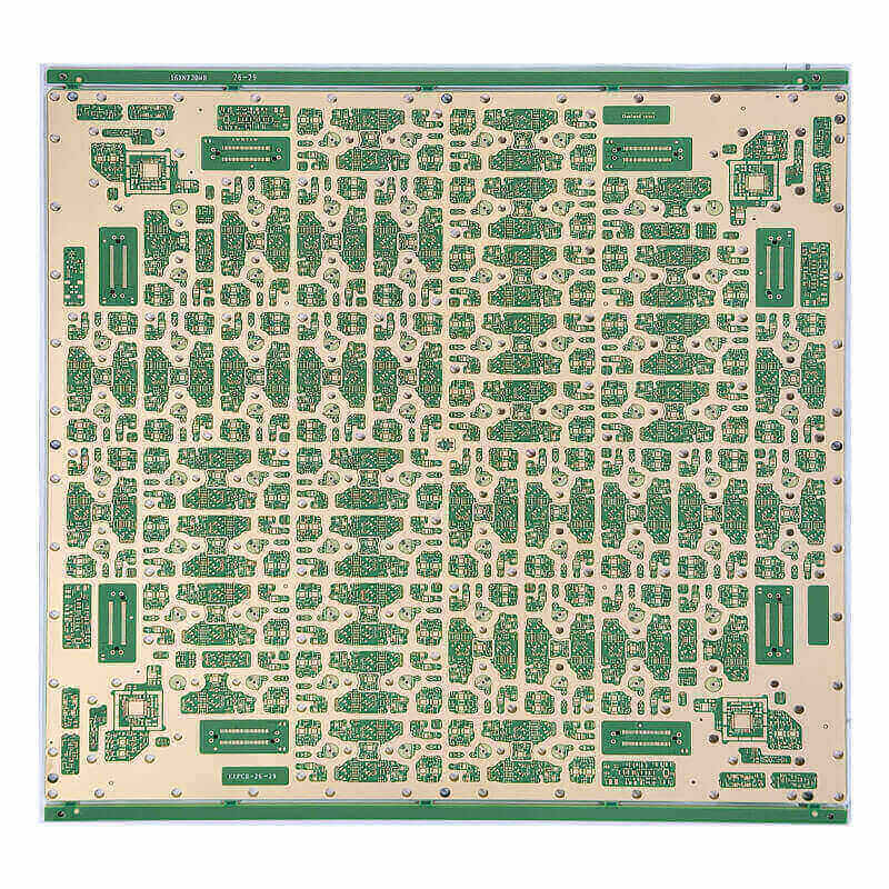
A pad connected to a plane with solid copper conducts heat away as fast as an iron or a reflow profile can deliver it. The joint then needs more energy and more time, which damages laminates and components and produces cold or incomplete fillets. Thermal relief design breaks that solid connection into narrow spokes so the heat path is restricted while the electrical connection remains acceptable.
The trade-off is deliberate. Every spoke that slows heat flow also adds a little inductance and resistance, and it reduces the copper cross section that carries current away from the pad. For a signal pad the penalty is negligible. For a ground pad carrying several amperes, or for a pad that must conduct heat into the plane, the relief can become the weakest point in the design and must be assessed rather than copied.
Balancing Spoke Width, Length and Count
Four spokes at 90 degrees is the common default because it is symmetric and easy to generate. Spoke width is the real control: wider spokes solder like a solid connection, narrower spokes slow heat enough to help but still deliver adequate current. Where a plane on an inner layer supplies the pad, the same rule applies through the via pattern, so the spokes and vias should be considered together rather than separately.
For hand soldering and repair, generous reliefs make the technician’s life easier. For automated reflow, the whole board is heated at once, so aggressive reliefs matter less and current carrying capacity matters more. The right choice depends on the assembly route, which is why the relief style should be stated on the fabrication drawing instead of left to the CAD default.
Wicking in Through-Hole and Wave Soldering
Wave soldering drives molten alloy into plated barrels under pressure, and if the barrel-to-lead gap is loose the solder climbs. A clearance that is too generous is worse than one that is snug, because the capillary force is weaker and the fill is less controlled. Barrel plating quality matters as much as the gap, since rough or thinly plated walls change how the alloy advances.
Designers can limit wicking by keeping the annular ring modest, by avoiding traces that leave a plated hole on the component side at a shallow angle, and by specifying a solder mask tent on vias that do not need to be soldered. The hole copper guide explains how plating thickness and hole geometry interact with the solder volume that a barrel can accept.
Wicking Risks in Fine-Pitch SMD and Via-in-Pad
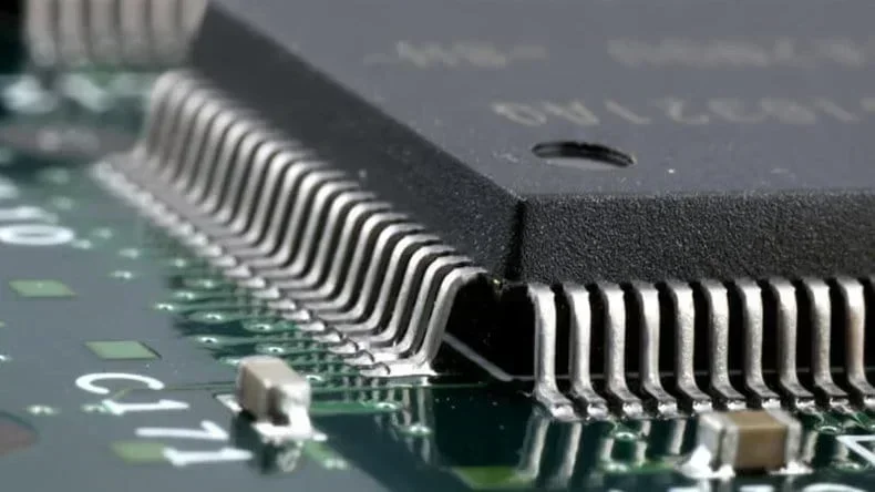
Fine-pitch packages place pads fractions of a millimetre apart, so any solder that leaves the pad has nowhere safe to go. Paste volume, stencil aperture and pad geometry decide whether the joint forms cleanly; exposed traces connected to the pad make the escape path easier. Keeping the trace width smaller than the pad, and masking everything else, limits how far a wick can travel.
Via-in-pad is the extreme case. An open via under a paste deposit will draw paste into the barrel during reflow, leaving the joint short of alloy and trapping flux residues inside the hole. The standard remedies are filling and plating over the via, or moving it out of the pad entirely. Both are fabrication decisions that have to be made before the artwork is released.
Copper Pour, Heat Sinking and Component Stress
Large copper areas are excellent heat sinking, which is why power devices, regulators and LEDs are placed on pours with many vias. The same property makes the pads around them hard to solder by hand and slow to reach temperature during reflow. If a small passive sits at the edge of a heavy pour, the pour pulls heat from the pad and the joint forms late in the profile.
The fix is not to remove the copper but to shape the connection. Reliefs on the small passive, a solid connection for the power device, and a deliberate gap between the two regions give each component the thermal environment it needs. Copper balance also matters for the panel, and the thieving and balance guide shows how the etch process reacts to uneven copper weights.
Designing Reliefs for Automated Assembly
Automated lines prefer consistency. If some ground pads are solid-connected and others have four spokes, the reflow profile that suits one will be wrong for the other. A single rule, applied across the board and recorded in the fabrication notes, gives the process engineer a predictable thermal load and removes a whole class of assembly defects from the discussion.
Note the intended relief style explicitly. Unconnected pad shapes generated automatically by CAD tools often use spoke widths that bear no relation to the assembly route, and the mistake is invisible on a schematic. Production notes that state spoke width, spoke count and the pads that must stay solid prevent the fabricator and the assembler from guessing.
Rework, Repair and Field Service
Repair is the hardest thermal case. A technician with a hand iron has far less energy available than a reflow oven, and a pad tied to a plane can absorb everything the iron delivers. Boards that must be serviceable should use slightly narrower spokes on connector and socket pads, and should keep a resist-free thermal path where a preheater or hot air tool can be applied.
Wicking also makes repair harder in the other direction. Solder that has crept along a trace leaves a thin coating that is difficult to remove and that can reflow unexpectedly, bridging neighbouring pads. Designing generous clearances and keeping sensitive nets away from heat sources reduces the amount of rework needed in the first place.
Inspection, Test and Common Failures
Visual inspection catches incomplete fillets and solder that has climbed a barrel, but it does not reveal voids inside a joint that was starved by wicking. X-ray shows the fill level and the voids, and it is the only practical way to confirm that a via-in-pad joint or a large ground pad is properly formed. Inspection criteria should be agreed before the first build.
When a board fails, the same failures recur: starved joints on ground pads, solder bridging between fine-pitch pins, and thermal damage to components that needed excessive heat. The solder defect review groups these by cause, and nearly all of them trace back to the pad-to-plane geometry that was fixed at layout time.
Documenting the Rules for Fabrication
Relief and wicking rules belong in the documentation package, not in a designer’s memory. State the thermal relief style, the spoke width, the pads that require solid connections, the vias that must be tented or filled, and the finish that will be used, since finish choice changes how solder wets and spreads during the first reflow pass.
A short note costs a few minutes and prevents a build that meets every dimension but solders badly. The fabrication notes checklist is a reasonable template. gopcb reviews these notes together with the artwork, because a relief that works on an inner layer may not work on an outer one, and the difference is visible only in the stack-up.
FAQ
Should every ground pad have a thermal relief? No. Power devices that must conduct heat into the plane should be solidly connected, and pads carrying high current need the full copper cross section. Reliefs are for pads that must be soldered individually.
Does a thermal relief weaken the ground connection? It adds a small amount of inductance and resistance, which matters only above a few megahertz or at high current. On a power plane carrying several amperes, verify the spoke cross section rather than assuming the default is adequate.
How do I stop solder wicking into via-in-pad? Fill and plate over the via, or move it out of the pad. Solder mask alone will not hold back paste during reflow, and the resulting void is usually discovered only by X-ray after assembly.