
PCB Warpage: Causes, Measurement and Prevention
Board warpage is one of the few defects that is visible before any component is fitted, and yet it is frequently reported late, because a panel that looks flat on the bench can bow by a millimetre once it has been through a reflow oven. Understanding where the curvature comes from makes it predictable rather than mysterious.
What Warpage Actually Is
Warpage is a permanent change in the shape of a board after the manufacturing stresses have been released, and it is measured against a flat reference plane rather than against a machine table. The standard method places the board on three supports and measures the deviation at the remaining points, which is why a board that is flat on a granite surface can still fail the measurement.
The measurement is normally expressed as a percentage of the diagonal for a bow, and as a percentage of the edge length for a twist. Both are specified because the two modes behave differently in assembly, and a board that is twisted will rock on a flat surface while one that is bowed will not.
Where the Stress Comes From
The stress is built in during lamination and released later. As the resin cures it shrinks, and it shrinks differently where it is bonded to copper than where it is bonded to laminate. If one layer of the stack contains a large area of copper and the layer opposite contains almost none, the two sides contract by different amounts and the board curves toward the copper-poor side.
The second source is the drilling and plating process, where a panel that is heated and cooled repeatedly accumulates its own stress pattern. The third is thermal, and it is the one that appears during assembly: a board that is flat when it arrives can bow the first time it passes through reflow. Our copper balance notes describe the pattern rules that control the first of these.
Copper Balance and Its Limits
Balance is judged in three ways: within a layer, between the layers of a core, and between the two halves of the finished stack. A layer that is dense in one corner and empty in another is unbalanced even if its total copper area matches the layer opposite, and the local imbalance is what produces a saddle shape rather than a simple bow.
The remedy is a thieving pattern, which is a grid of isolated copper features added to the sparse regions until the distribution is uniform. The pattern is usually specified as a percentage of area, and the target is a difference of a few per cent between the two sides of a core.
Stack Symmetry
A stack that is not symmetric about its centre line will warp, because the two halves shrink by different amounts as they cool. Symmetry means matching not only the number of layers but also the dielectric thickness, the copper weight and the construction of each core, so a stack built as two separate cores on one side and a single core on the other is asymmetric even if it has an even number of layers.
That is the practical reason for preferring symmetric constructions, and it is why a design that adds a layer for routing reasons is often better served by adding two. Our layer assignment notes describe how a balanced stack is built.

Material Choice and Warpage
The laminate’s glass transition temperature and its coefficient of thermal expansion both affect how much the board moves when it is heated. A material with a high glass transition temperature keeps its stiffness at reflow temperature, so it deforms less, while a standard material softens and takes a set.
The reinforcement also matters. A laminate with a woven glass fabric behaves differently along the warp and weft directions, and a board whose outline is aligned with neither will twist when it is heated. Our laminate material notes describe the properties to confirm.
Board Thickness and Aspect Ratio
A thin board warps more than a thick one for the same stress, because stiffness rises with the cube of the thickness. That is why a large, thin board is the hardest case to keep flat, and why the combination of a large outline and a thin finished thickness is worth questioning at the design stage.
Where a thin board is unavoidable, the panelisation should be arranged so that the boards are supported during processing, and the assembly carrier should be considered before the design is released rather than after the first batch warps.
Assembly and Handling Effects
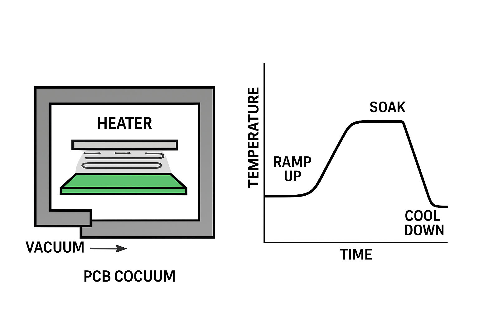
Warpage that appears during assembly usually comes from an uneven thermal profile. A board that is hotter on one edge than the other expands unevenly, and if it is clamped at that moment the stress is locked in. Preheating the assembly evenly and supporting it through the oven reduces the effect.
Handling matters too. A board that is bowed by hand while it is hot will take a permanent set, and the damage is not visible until the board cools. The relevant control is straightforward: no manual handling of a board above the glass transition temperature of its laminate.
Correcting a Warped Board
Baking a board above its glass transition temperature under a flat weight can flatten it, and the result is acceptable for some applications and not for others, because the process changes the material’s state and may affect the dimensional stability of the finished board.
Where warpage must be corrected, the decision should be made with the customer, and the corrected boards should be measured again rather than assumed to be flat. Our board quality notes describe how the measurement is recorded.
Process Control and Verification
Reviewing the design before the data is released is far cheaper than correcting it after the panel is in the tank, because every step downstream inherits the decision made at the front end. Where a value sits close to a process limit, the drawing should say so, since the shop can then open the process window rather than working to a nominal figure that carries no tolerance.
The measurements that matter are the repeatable ones: conductor width and spacing, annular ring, finished hole size, plating thickness and surface finish are all verifiable on a coupon that travels with the panel. Documenting the assumption is part of the design work, and a short note on the drawing prevents a question that would otherwise arrive a day later and cost a day of schedule.
Where a value sits close to a process limit, the drawing should say so, since the shop can then open the process window rather than working to a nominal figure that carries no tolerance. Running a first article through the same checks as the production panel confirms that the two agree, and that comparison is the cheapest form of process control available at prototype stage.
FAQ
What warpage figure is acceptable? The common specification is a fraction of a per cent of the diagonal, with a tighter figure for boards that will be assembled with fine-pitch components. The requirement should come from the assembly process rather than from a default, because the flatness that a placement machine needs is the figure that matters.
Can warpage be predicted before the board is built? Approximately. A stack with a balanced copper distribution, a symmetric construction and a material whose properties are known will usually come out flat, and a stack that fails any of those tests usually will not. Running the check at the stack-up stage costs nothing and prevents a batch of curved panels.
What does gopcb do about warpage? We check the copper balance of each layer before the panel is released, confirm the symmetry of the stack, and measure the finished board against the specification. Where the measurement is close to the limit we report it with the shipment rather than waiting for the customer to find it.