PCB Manufacturing Cost Waste: Where Money Is Lost
Cost waste in board production rarely appears as one dramatic mistake. It accumulates as scrap on a panel, rework on a line, an expedited shipment and a specification that is higher than the application requires. Each item looks small in isolation, and together they can account for a significant share of the unit price. This guide examines where pcb manufacturing cost waste actually occurs and how to remove it.
What Cost Waste Actually Looks Like
Waste has four common forms. Material is lost when a panel is not fully used or when boards are scrapped after processing. Time is lost when a board is reworked or when a line waits for a decision. Money is lost when an order is expedited unnecessarily. Capability is lost when a specification demands a process the product does not need.
None of those appear as a line item on an invoice, which is exactly why they persist. A quotation shows the price; it does not show the margin that was consumed producing the part. Identifying where the money goes requires looking at the process rather than at the price list.
Panel Utilisation and Material Loss
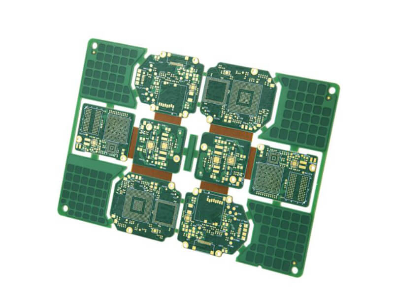
Panel utilisation is the most measurable form of waste. The fabricator buys a standard panel and fills it with circuits, so any area left unused is purchased material that produces nothing. A layout that tiles efficiently uses most of the panel, while an awkward outline or an odd dimension wastes a strip on every side of every circuit.
The waste multiplies with quantity. A five percent loss on a hundred panels is a rounding error; the same loss on ten thousand panels is a significant amount of laminate, copper and processing time. Improving layout decisions that affect production is therefore a volume-scale saving rather than a cosmetic one.
Design Decisions That Raise the Scrap Rate
Some designs are simply harder to build, and difficulty shows up as scrap. A trace width close to the process limit, a pad that is smaller than the standard annular ring, or a solder mask dam that is too narrow all reduce the process window. The board can be built, but only with a tighter setup and a higher reject rate.
The cost of that difficulty is charged inside the unit price rather than separately, which makes it easy to miss. Applying design for manufacturability rules is not a formality; it is the difference between a design that runs on any line and one that runs on the best line only.
Rework Cost and Its Hidden Multiplier
Rework cost is usually underestimated because only the labour is counted. The real cost includes the operator time, the replacement components, the risk of damage during removal, the second inspection and the loss of schedule. A rework operation that takes ten minutes can consume an hour of total capacity.
On a complex assembly the multiplier is larger, because removing a fine-pitch component risks the pads underneath it and may turn a repairable board into scrap. Reducing rework is therefore as much a design objective as reducing component count, and the same principles of board quality apply to both.
Schedule Pressure and Expedited Spending
Expedited shipments are often treated as a logistics cost when they are really a planning failure. If a board is ordered late because an approval was delayed, the premium buys fabrication time that cannot recover the lost week. The waste is the premium itself, and it was avoidable at the point where the delay occurred.
Schedule pressure also creates technical waste. A rushed build has less time for a first-article review, so a marginal process issue is more likely to reach production. The cost of that is not visible in the expedited invoice; it appears later as a yield problem on the following order.
Specification Inflation
Specification inflation is the quietest form of waste. A laminate chosen for a temperature range the product will never see, a finish specified for a shelf life that will not be used, or an impedance tolerance tighter than the signal requires all add cost without adding function. Each individual step looks defensible; together they raise the price noticeably.
The remedy is to derive the specification from the application. Recording the actual temperature, humidity, life and signal requirements in the design file makes it possible to challenge a specification later, and it turns a set of habits into a set of decisions.
Measuring Waste Before Removing It
Waste cannot be managed without measurement, and the simplest measurement is a comparison. Price the same design at two panel utilisations, or ask for the yield assumption behind a quotation. A supplier who can state the assumed scrap rate is describing a process rather than guessing at a number.
A second useful measure is the number of design changes after the first order. Each change resets tooling, test programmes and approvals, so the count is a proxy for rework and for the cost it will generate. Reducing that count is usually the highest-value improvement available to a hardware team.
Practical Steps That Remove Waste
Start with geometry: improve the nesting, keep the outline simple, stay on a standard thickness and use the lightest copper that satisfies the current. Then review the process window: widen the fine features where possible, respect the standard annular ring and keep the mask dam within the supplier’s capability.
Finally, plan the schedule. A rolling forecast, a small buffer of finished boards and a realistic approval timeline remove most expedited spending. None of those steps requires new technology, and together they address material loss, scrap, rework and premium freight at the same time.
Process Control and Verification
Reviewing the design before the data is released is far cheaper than correcting it after the panel is in the tank, because every step downstream inherits the decision made at the front end. Where a value sits close to a process limit, the drawing should say so, since the shop can then open the process window rather than working to a nominal figure that carries no tolerance.
The measurements that matter are the repeatable ones: conductor width and spacing, annular ring, finished hole size, plating thickness and surface finish are all verifiable on a coupon that travels with the panel. Documenting the assumption is part of the design work, and a short note on the drawing prevents a question that would otherwise arrive a day later and cost a day of schedule.
Where a value sits close to a process limit, the drawing should say so, since the shop can then open the process window rather than working to a nominal figure that carries no tolerance. Running a first article through the same checks as the production panel confirms that the two agree, and that comparison is the cheapest form of process control available at prototype stage.
FAQ
What is the single largest source of waste in PCB production? Panel utilisation in most cases, because it affects material and processing time together and it scales with the order size. It is also the easiest to influence, since it is decided at layout stage.
Does a tight specification always cost more? Not always, but it usually does. A tolerance or material that the product does not need narrows the process window, and a narrower window means a lower yield and a higher unit price on every order.
How can a small team reduce waste? By measuring two numbers: the design changes after the first order and the yield assumption in the quotation. Improving either of them reduces scrap, rework and expedited spending without any change to the product.