Non-Layered PCB: A Guide to Single-Layer Boards
A non-layered PCB carries a single copper layer on an insulating base, and its simplicity is the whole point. It is the cheapest board that can be manufactured at volume, it is fast to build, and for a large class of products it is entirely sufficient. This guide explains the construction, the cost structure and the design limits of the format.
What a Non-Layered PCB Is
The format is also the fastest to tool. There is no lamination cycle, no plating line and no inner-layer registration, so a new design can be released and built in a fraction of the time a multilayer board requires. For a product with a short development window, that speed is worth as much as the unit price.
A non-layered PCB, also called a single-layer board, has one conductive layer on one face of the substrate. Components are mounted on that face, connections are made by etched conductors, and any connection to the other side is made by a through-hole component lead rather than by a plated via.
That is the defining difference from a double-sided board. Without plated through-holes there is no electrical path between faces, so the format is really a one-sided circuit with mechanical mounting on the reverse. It is the oldest PCB construction and remains the cheapest.
Structure and Key Elements
Four elements make up the board: the substrate, the copper foil, the solder mask and the legend. The substrate is usually a paper or glass-reinforced laminate chosen for cost and mechanical rigidity, the copper is laminated to one face and etched into the pattern, and the solder mask protects the conductors except at the joints.
The copper foil thickness sets the current capacity and is specified as an ounce weight. One ounce is the common default, and heavier foil is used where the traces carry more current. The pattern itself is defined by the circuit, and the pad design standards that apply are the same as on any other board.
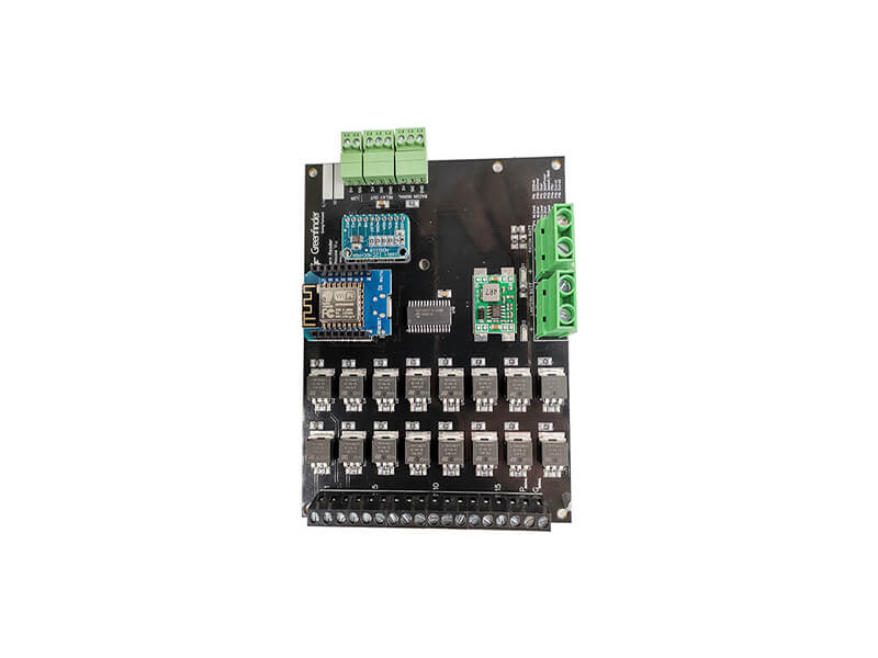
Where Single-Layer Boards Make Sense
Single-layer construction suits circuits with a modest component count and no need for a ground plane: small appliances, toys, LED lighting, simple power supplies and basic sensor modules. It also suits products with a high production volume, because the tooling cost is low and the process is short.
It is a poor fit for anything with a controlled impedance requirement, a dense fine-pitch package or a need for a continuous return path. Those requirements are not difficult to meet; they simply cannot be met on a single conductive layer, and attempting it produces a design that works on one bench and not on the next.
Cost Structure and Volume
The pcb manufacturing cost of a single-layer board is dominated by area and by the number of drilled holes rather than by the circuit itself, since the pattern is defined in one etch step. That makes it a useful reference point when comparing quotations, because it removes most of the process variables that confuse a multilayer comparison.
Cost is dominated by material and handling rather than by process time. The fabrication sequence is short, the yield is high, and the main variable is how many boards fit on a panel. A non-layered board is therefore a panel utilisation exercise more than a technology exercise.
Volume changes the picture less than it does on a multilayer board, because there is little setup to amortise. The cheapest unit price arrives early, and the difference between a thousand boards and ten thousand is smaller than a designer might expect.

Design Limits and Routing Constraints
Jumper links are a legitimate tool rather than a failure. A zero-ohm resistor or a wire link resolves a single crossing at negligible cost, and a design using two or three of them may still be cheaper than moving to a double-sided board. Beyond a handful, the trade reverses.
The single copper layer means every net has to reach its destination without crossing another net. That is achieved by routing around obstacles, by using zero-ohm links or wire bridges, and by accepting a longer path than the schematic would suggest. Dense designs quickly become impossible.
Clearance is the other constraint. A single-sided board cannot use an inner plane to solve a spacing problem, so the copper-to-edge distance and the spacing between adjacent conductors have to be planned on the one available layer. Applying manufacturable design guidelines keeps those distances inside the process capability.
Standards, Compliance and Safety
A single-layer board is subject to the same safety and environmental requirements as any other. Creepage and clearance still apply to mains-referenced circuits, flame retardancy requirements still apply to the laminate, and the finish still has to be compatible with the soldering process and any restriction on materials.
The difference is that the layout has fewer tools available to meet those requirements. Where a multilayer board can solve a spacing conflict by moving a net to another layer, a single-sided board has to solve it in two dimensions, which usually means more area or a smaller feature size.
Assembly and Test
Panel design matters here as much as anywhere. A single-sided product is often assembled on a panel and separated afterwards, so the tabs, the rails and the fiducials have to suit the placement equipment. Skipping them forces the assembly house to handle loose boards, which is slower and less reliable.
Assembly is straightforward when the design uses through-hole parts, because the copper face can be wave soldered in one pass. Where surface-mount parts are used, the board is usually a single-sided assembly in the literal sense as well, which removes a second reflow and its handling step.
Testing is normally a simple electrical check plus a visual inspection. There are no inner layers to verify and no impedance to measure, so the acceptance criteria are short. That is one reason the format is popular for high-volume, low-cost products.
When to Move to Two Layers
The underlying principle is the same as on any PCB construction: the board should be no more complex than the circuit requires, and no simpler either. Choosing the layer count from the routing and the reference requirement rather than from habit keeps both cost and risk under control.
The move to two layers is triggered by one of three things: a net that cannot be routed, a need for a ground reference, or a component that requires a plated through-hole. Any of those makes a double-sided board cheaper than the workaround it would otherwise require.
The decision should be taken early rather than late. Adding a second layer at layout stage costs a modest amount; reworking a single-sided design after it fails an EMC test costs considerably more, because the fix usually involves more than the layer that was saved.
FAQ
Is a non-layered PCB the same as a single-sided PCB? They are the same construction. The terms describe a board with one conductive layer, as opposed to a double-sided or multilayer board, and the distinction matters mainly for routing and for plated through-holes.
Can a single-layer board have plated holes? Plated through-holes require a second conductive surface to connect to, so a true single-layer board does not use them. Component leads pass through unplated holes and are soldered on the copper side.
How much cheaper is a single-layer board? It is the cheapest fabrication option per unit area, but the gap narrows at high volume because the setup charges on a two-layer board are amortised. The larger saving is usually in assembly, not in fabrication.