




PCB Circuit Board Explained: Materials, Design and Process
A printed circuit board is the physical carrier of an electronic design. It holds the components, connects them electrically, removes the heat they generate and provides the mechanical structure that lets the product survive handling. Each of those functions is performed by a different part of the board, and understanding what those parts are makes the design decisions that follow much easier to reason about.
What the Board Is Made Of
The base material is the structural core. In most products it is a glass fibre reinforced epoxy laminate, commonly FR-4, which provides mechanical support and electrical insulation between conductors. Variants exist for particular requirements: aluminium-backed material where heat must be conducted away, polyimide where the board must flex or tolerate high temperature, and high-frequency laminates where the dielectric loss at microwave frequencies has to be low.
Copper foil is the conducting layer, bonded to the base material and patterned into traces, pads and planes. Its thickness determines how much current a trace can carry and how much heat it spreads, and it is specified in ounces per square foot, with one ounce corresponding to about 35 micrometres. Heavy copper constructions are available where the current demand or the thermal load requires them.
The solder mask is the polymer layer printed over the copper, exposing only the areas that must be soldered. It prevents solder from bridging between adjacent pads, protects the copper from oxidation and contamination, and provides electrical insulation across the surface of the board. Its formulation and its printing behaviour are discussed in this article on solder mask ink thixotropy.
Both layers are thin relative to the copper, but neither can be omitted without consequence. A mask that does not adhere, or that flows into a pad opening, becomes a soldering defect; a silkscreen printed over a pad becomes a barrier to the joint.
`r`n
The silkscreen is the printed legend on the surface, used to identify components, orientation marks and test points. It carries no electrical function, but a board without a useful silkscreen is difficult to assemble and almost impossible to repair. It must not overlap pads that will be soldered, and its minimum line width follows from the printing process.
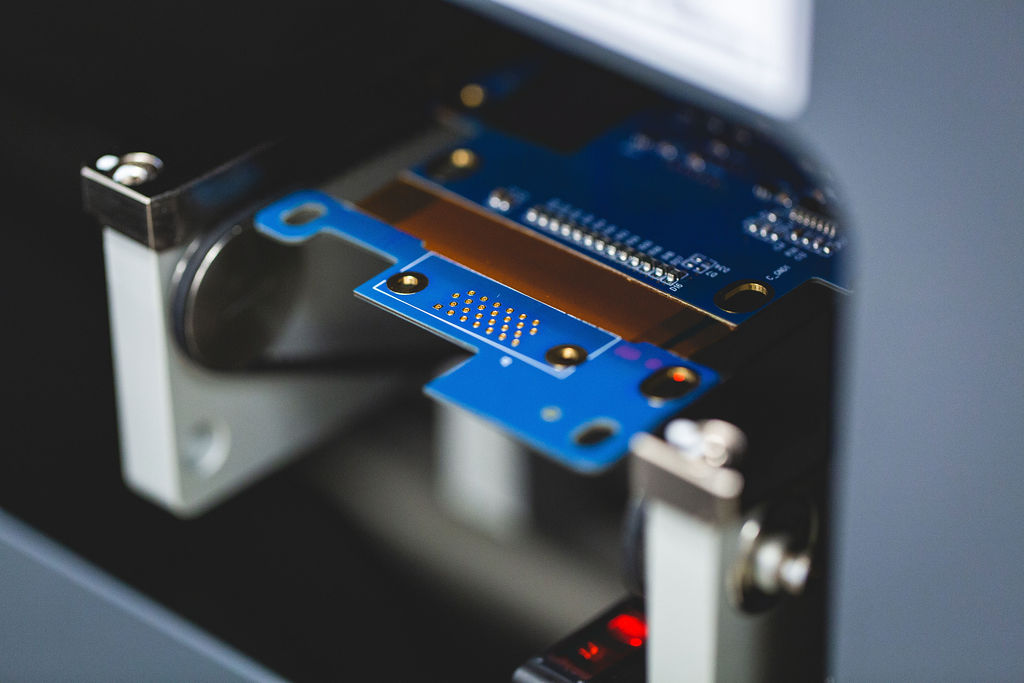
How the Layers Are Built Up
A single-sided board carries copper on one surface and is suitable only for the simplest circuits. A double-sided board carries copper on both, connected by plated through holes, and it is the first format in which a ground plane becomes practical. A multilayer board sandwiches additional conducting layers between insulating ones, joined by plated vias, and it is the format used by anything digital at speed.
The arrangement of those layers, and the principles that determine which layer should carry signals and which should carry planes, are the subject of this discussion of layer stackup design. The thickness of the finished board, the dielectric constant of the material and the copper weight on each layer are all fixed at this stage, and changing any of them later invalidates the impedance calculations and the mechanical design.
From Schematic to Layout
Design begins with the schematic, which expresses the logical connections between components without saying anything about their physical position. The netlist derived from the schematic is the input to the layout, and every subsequent step depends on it being correct. A netlist error is far cheaper to find before the board is routed than after.
Placement follows. Components are positioned so that the critical connections are short, the functional blocks are separated, the mechanical constraints are respected and the assembly process can reach every joint. Placement determines the length of every trace and the thermal environment of every part, so it has more influence on the finished performance than the routing that follows.
Routing connects the components, and it is where the electrical requirements meet the manufacturing limits. Trace widths are set by current and impedance, spacing is set by crosstalk and by the fabricator”s capability, and the geometry around pads and holes is set by the assembly process. The rules governing the geometry around pads and holes, and the clearance that must be left between them, are described in this article on PCB pad design standards.
Component Placement and Routing Principles
Several placement principles apply to almost any design. Connectors and other mechanical parts are fixed by the enclosure and should be placed first. Sensitive circuits are placed away from noise sources. Components that dissipate heat are placed where the heat can escape, which may mean the edge of the board or a region with a thermal path through vias to the other side. Parts that belong to the same functional block are grouped together so their interconnections are short.
The routing principles follow the same logic. Signals are routed over a continuous reference, and the reference is checked before the route is accepted rather than after. Fast nets are kept as short as the placement allows, and they are assigned to the layers with the best reference. Different nets are kept apart, particularly where a sensitive trace runs beside a switching one, and the spacing that achieves that is described in this discussion of the 3W rule.
Throughout, the fabrication limits constrain what is possible. Minimum trace and space, minimum hole size, the aspect ratio of a plated hole, the accuracy of layer registration and the panel construction all determine what the fabricator can build. A design that ignores any of them may pass every electrical check and still be unbuildable at the quoted price.
The Manufacturing Sequence
The board is fabricated layer by layer. Inner layers are imaged and etched, the layers are stacked with insulating material between them and laminated under heat and pressure, holes are drilled, copper is plated into the holes and onto the surface, the outer layers are patterned, the solder mask and silkscreen are printed, and the surface finish is applied. Each step contributes its own tolerance, and the ones that affect hole position relative to copper are described in this article on via to trace clearance.
Assembly then follows: paste is printed through a stencil, components are placed, the assembly is reflowed, and any through-hole parts are inserted and soldered. The finished assembly is tested, and the test strategy determines which nets must remain accessible.
FAQ
What is the difference between a PCB and a PCBA? A PCB is the bare board with copper, mask and silkscreen but no components. A PCBA is that board after the components have been placed and soldered. The design work is the same, but the assembly constraints apply only to the PCBA.
Why does copper thickness matter? It determines how much current a trace can carry without overheating and how effectively the copper spreads heat away from a component. It is specified in ounces, with one ounce equal to about 35 micrometres of copper, and it is fixed per layer at the time the stackup is chosen.
What is the silkscreen for if it carries no current? Identification. It shows where components go, which way they face, and where test points and connectors are. A board without a clear silkscreen is harder to assemble and much harder to repair, so it is treated as a functional requirement rather than decoration.



1 Comment
5 Key Stages of PCB Prototype Manufacturing
[…] an open at this stage costs a repair; catching it after assembly costs the components as well. The basics of a circuit board explain why the netlist, not the visual appearance, is the reference for this […]