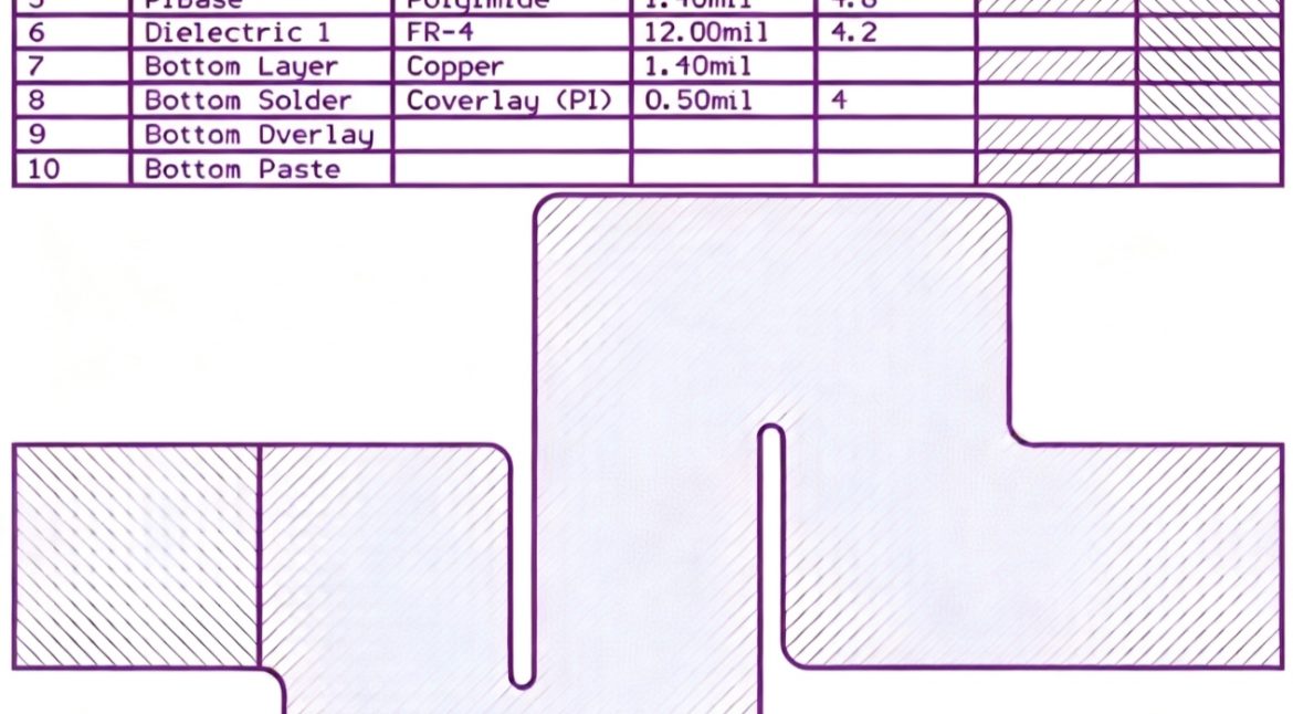
Thermal Via: Thermal Path Design From Junction to Ambient
Heat is the enemy of every electronic product up to a point, and beyond that point it is the friend. Most failures in service are thermal in origin, and most of them are decided by the path the heat takes from the junction to the ambient, which is a mechanical and a material question as much as an electrical one.
The Path From Junction to Ambient
Heat leaves a semiconductor through the die attach, the lead frame or the substrate, the solder joint, the pad, the board and finally the air or the enclosure. Each of those steps has a thermal resistance, and they add in series just as electrical resistances do.
The largest single resistance is usually the last one, the path from the board surface into the air, which is why a component that runs hot on a bare board often runs cool once it is fastened to a metal chassis. The design question is which resistance dominates, because improving any other one has no effect.
Thermal Vias and Their Limits
A thermal via array moves heat through the board by conduction, and the array is effective in proportion to the copper cross-section it presents. Twenty small vias outperform five large ones of the same total area, because the plating thickness is limited and many small barrels give more copper than a few large ones.
The limit is the dielectric between the vias and the thermal resistance of the plane beneath. An array that pours heat into a plane that cannot spread it simply moves the bottleneck. Our thermal management notes describe how the array is sized.
<img src="https://www.gopcba.com/wp-content/uploads/2025/08/26.png" alt="Thermal image of a PCB showing heat spreading from a power device” />
Copper Weight and Spreading
Copper spreads heat laterally, and a heavier layer spreads it over a wider area, which reduces the temperature at any single point. This is one of the few cases where increasing the copper weight has a direct thermal benefit that is easy to calculate.
The spreading is limited by the area available, so a design that concentrates all the heat-generating components in one corner will see a hot spot whatever the copper weight. Distributing them, or providing a dedicated thermal plane, is usually more effective than increasing the thickness of a layer that is already there. Our metal core notes compare the alternatives.
Interface Materials
Where a component is fastened to a heatsink, the interface between them is filled with a material that displaces the air. Air is a good insulator, so even a thin layer of it dominates the thermal resistance across the joint, and the purpose of the interface material is simply to remove it.
The material has its own resistance, which is why the thickness matters as much as the conductivity. A thin layer of a moderate material usually outperforms a thick layer of an excellent one, and the clamping force that determines the thickness is part of the thermal design.
Convection and Its Dependence on Orientation
Natural convection depends on the orientation of the surface, because the buoyancy that drives the airflow is aligned with gravity. A vertical board sheds heat more effectively than a horizontal one, and a board mounted horizontally with the hot side facing down is the worst case.
Where the product can be mounted in more than one orientation, the thermal design should be verified in the worst case rather than in the one that is convenient to test. This is a common source of field failures in products that were qualified in a laboratory orientation.
Thermal Cycling and Mechanical Stress
Temperature changes produce mechanical stress, because the materials in an assembly expand by different amounts. The stress is concentrated at the interfaces, and it accumulates over cycles until a crack forms or a joint fails.
The design response is to reduce the constraint: use compliant joints, avoid large rigid areas bonded to materials with different expansion, and keep the temperature excursion as small as the application allows.
Measuring the Thermal Path
A thermal image shows where the heat is, and a thermocouple shows how hot a point becomes, but neither explains why. To understand the path, the resistances have to be estimated and the largest one identified.
The estimate does not need to be precise. Knowing that the joint contributes a tenth of the total resistance and the convection contributes half is enough to direct the effort to the right place, and it takes a few minutes with published material data.
Designing for Manufacture and for Service
A thermal solution that requires a special assembly step is a manufacturing cost, and one that cannot be disassembled is a service cost. Both should be considered at the design stage, because a heatsink that is bonded with a permanent adhesive makes a field repair impossible.
Where the product has to be serviceable, the thermal path is usually re-established through a removable interface rather than an adhesive. The small loss in thermal performance is the price of being able to repair the unit. Our industrial systems notes describe the related requirements.
Process Control and Verification
Reviewing the design before the data is released is far cheaper than correcting it after the panel is in the tank, because every step downstream inherits the decision made at the front end. Where a value sits close to a process limit, the drawing should say so, since the shop can then open the process window rather than working to a nominal figure that carries no tolerance.
The measurements that matter are the repeatable ones: conductor width and spacing, annular ring, finished hole size, plating thickness and surface finish are all verifiable on a coupon that travels with the panel. Documenting the assumption is part of the design work, and a short note on the drawing prevents a question that would otherwise arrive a day later and cost a day of schedule.
Where a value sits close to a process limit, the drawing should say so, since the shop can then open the process window rather than working to a nominal figure that carries no tolerance. Running a first article through the same checks as the production panel confirms that the two agree, and that comparison is the cheapest form of process control available at prototype stage.
FAQ
How many thermal vias are enough? Enough that the vias do not become the dominant resistance in the path. A useful starting point is to match the copper cross-section of the vias to the area of the thermal pad, which on a typical design means an array filling the pad on a regular pitch rather than a few vias around the edge.
Does a heatsink always help? It helps when the limiting resistance is the path from the board to the air. Where the limit is inside the component or at the solder joint, a heatsink adds cost and mass without changing the junction temperature, and the effort should go into the joint instead.
What does gopcb check on a thermal design? We check the copper area beneath the heat-generating components, the thermal via array and its connection to the plane, the thermal relief on soldered joints, the copper balance of the stack and the flatness of the board, since a warped board will not sit against a heatsink properly.