Balanced Copper in PCB Design
A finished panel that is not flat is difficult to assemble and impossible to solder reliably. The board may bow along one axis, twist about a diagonal, or simply refuse to sit flat in a fixture, and the cause is usually the way copper was distributed across the layers rather than anything that happened in the press. Balanced copper is the design habit that prevents it.
Why Copper Balance Matters
Copper and laminate expand at different rates when heated, and they shrink at different rates when cooled. During lamination, the stack is pressed at high temperature and then cooled under pressure, and each layer tries to move by a different amount. If the copper on the two sides of a core is unequal, the two sides behave differently and the core curls.
The effect is cumulative. A stack of cores each with a slight imbalance produces a panel with a pronounced one, and the distortion appears only after the panel is cooled and the pressure released, which is why it is often a surprise during a later process step rather than during lamination itself.
How Unbalanced Copper Causes Bow and Twist
Bow is a curvature along one axis, with the centre of the board displaced from the plane defined by the corners. Twist is a rotation about a diagonal, with one corner out of plane while the others remain. Both are measured against a reference plane and both are specified as a percentage of the board dimension in most acceptance standards.
The mechanism behind them is the same. Uneven copper produces uneven shrinkage, and the residual stress that remains locked in the panel is released as curvature. Thin boards, large panels and high layer counts all make the effect more visible because there is less material to resist it.
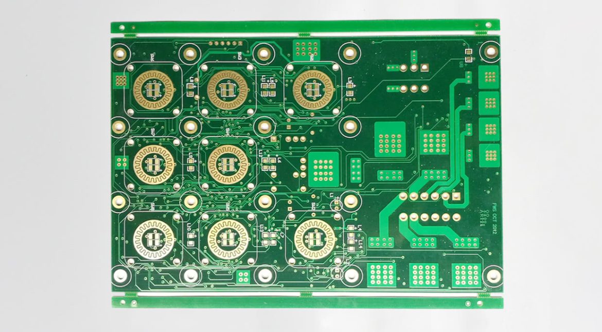
<img src="https://www.gopcba.com/wp-content/uploads/2020/04/ptt_service-1.jpg" alt="PCB layers with balanced copper distribution across the panel” />
Copper Distribution Across a Panel
The distribution question is about the whole panel, not about a single board. A panel with one dense board and one sparse board will behave differently from a panel of uniform boards, and the difference is large enough to affect the yield of the boards at the edges. Where the panel contains different products, the imbalance is unavoidable and has to be managed by other means.
On the same board, the layers themselves should balance. A layer that is 80 percent copper on one side of a core and 30 percent on the other is a design decision that produces a warped core, and it is easy to create accidentally when a power plane is paired with a sparse signal layer.
The Effect on Lamination
Lamination is where the imbalance becomes permanent. The resin flows to fill the spaces between copper features, and the amount of resin that must flow depends on the copper density. Areas with little copper need more resin movement than areas with a lot, and the resulting variation in thickness changes the dielectric constant and the impedance of the traces in those areas.
Our notes on PCB lamination process guide describe how pressure, temperature and resin flow interact, and why a stackup that looks balanced on paper can still press unevenly if the copper distribution varies sharply across a layer.
Design Techniques for Balance
The most direct technique is symmetry: keep the copper density of each layer close to that of the layer that mirrors it in the stackup, and keep the density of any single layer as uniform as the routing allows. Where the functional copper cannot be made uniform, the gaps can be filled with non-functional features such as a copper grid or thieving pads, which bring the density up without changing the circuit.
These features are not free. They add artwork, they take time to generate, and on a high frequency layer they can affect the electrical environment if they are placed carelessly. On a power or ground layer they are almost always beneficial, and it is worth being explicit about where they are wanted rather than applying them across the whole board.
Balance in Multilayer Stackups
In a multilayer board, balance is a property of the stack rather than of individual layers. The conventional rule is to build the stack symmetrically about its centre, matching dielectric thicknesses and copper weights on either side, and to keep the copper density of the layers symmetric in the same way.
Our notes on PCB dimensional stability and expansion describe how the material properties interact with the stack, and why a symmetric construction behaves better through the thermal excursions of assembly than an asymmetric one of the same total thickness.
Balance and Electrical Performance
Balance is usually discussed as a mechanical issue, but it has electrical consequences. Uneven resin flow changes the dielectric thickness and therefore the impedance of the traces in that area. Warp changes the distance between a surface trace and its reference plane, and it also affects how well a component sits on its pads during assembly.
There is also a manufacturing consequence for imaging. A distorted panel is harder to register accurately, so a board that is not flat tends to show more registration variation in its vias and pads. The two problems share a root cause and often appear together.
Measuring and Accepting Distortion
Distortion is measured by placing the panel on a flat surface and measuring the maximum deviation, expressed as a percentage of the board length. The acceptable value depends on the product and on the assembly process, and a board that passes the standard may still cause problems on a line that cannot tolerate any curvature at all.
The measurement should be taken after every thermal step, not only at the end, because a board that is flat after lamination can distort after reflow. Where a product has a tight requirement, it is worth agreeing the measurement method and the acceptance limit with both the fabricator and the assembler.
Working With the Fabricator
Balance is a design input that the fabricator can see and comment on, which makes the stackup review the natural point to discuss it. A fabricator who reviews copper density across the panel before the artwork is released can suggest thieving or a change in the layer pairing, and the suggestion costs nothing at that stage.
Our notes on prepreg versus core describe the material decisions that sit underneath the balance question, and how the choice of construction affects both the pressing behaviour and the finished thickness. At gopcb, stackups with asymmetric copper are flagged during review so that the balance is addressed in the design rather than in the press.
Additional Considerations for This Build
Practical attention to panel design pays for itself here, because it decides whether the finished board behaves as the drawing intended. Where the requirement is not stated on the fabrication drawing or in the assembly notes, the shop has to assume a default, and that default is rarely the value the design was simulated with. Stating panel design explicitly, together with the tolerance that applies, removes the assumption and keeps the result predictable from batch to batch.
FAQ
Does thieving copper change the circuit? No, provided the added copper is not connected to a net and is placed where it does not alter the impedance of a controlled line. It exists to make the layer press evenly.
Is a symmetric stackup always necessary? It is the simplest way to a flat board, but not the only one. An asymmetric stackup can be made to work if the copper densities are managed and the fabricator agrees to the construction.
Why did the board only warp after reflow? Because the lamination stresses were balanced enough at room temperature and the assembly heating released them. The distortion was always present in the panel as residual stress, and the second thermal cycle revealed it.