Connector Bandwidth: Where The Channel Really Ends
A channel is usually analysed as a trace with a driver at one end and a receiver at the other, and the connector is treated as a detail. At high data rates that treatment is wrong. The connector often contributes more loss and more reflection than the trace it interrupts, and its footprint on the board can be the largest single discontinuity in the path.
This article looks at what limits a connector’s bandwidth, how the footprint affects the channel, and how to evaluate a connector honestly rather than by its advertised data rate.
The reason connectors are difficult is that they are three dimensional structures with a ground system that does not resemble the transmission line on either side of them, so the transition has to be designed rather than assumed.
What Sets The Limit
Three mechanisms dominate. The first is inductance in the signal and return paths: the pin, the mating contact and the path through the connector body all add series inductance. The second is capacitance between adjacent contacts and between the contacts and the shell. The third is the impedance discontinuity where the wide footprint pad meets the narrow trace.
The result is a low pass characteristic. Series inductance and shunt capacitance form a filter, and the frequency at which it begins to remove energy depends on how those elements are distributed. A connector with a good ground system distributes the return close to every signal and pushes the corner frequency upward.
The Ground System Is The Specification
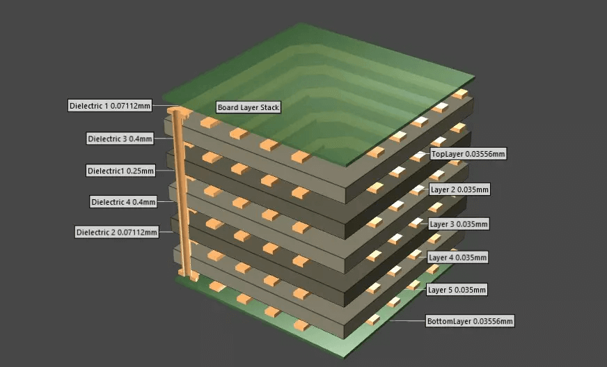
Manufacturers quote a data rate for a connector only when a defined number of contacts are assigned to ground and the pair assignments follow a recommended pattern. Using the same connector with a different ground assignment produces a different, usually worse, result. The ground pins are not spare contacts; they are the return path that makes the signal pins behave as transmission lines.
The consequence for the design is that the footprint must be used as intended. The recommended ground pattern should be followed, the pairs should be assigned to the contacts the manufacturer characterised, and the board stackup should be arranged so that the connector’s own ground structure connects to a plane with a short, wide path.
The Footprint: Where Most Of The Damage Happens
A connector footprint consists of pads that are wider than the trace and a region where the reference plane has been removed to avoid shorting to the shell or to the contacts. Both change the impedance. The wide pad adds capacitance, and the removed plane removes the return path, which adds inductance over the length of the void.
The usual remedies are to keep the plane as close to the pads as the connector allows, to add ground vias close to the signal pads so that the return has somewhere to go, and to taper the trace into the pad rather than meeting it abruptly. The via placement around the footprint is often what decides whether the transition is acceptable.
Measuring A Connector Honestly
The datasheet figure is measured in a fixture that may not resemble the application board, and the fixture itself contributes to the result. A more useful approach is to measure the assembled channel: connector, footprint and trace together, launched from a calibrated reference. The difference between that measurement and the same trace without the connector is the connector’s true contribution.
Where a full measurement is impractical, simulation of the footprint with the actual stackup is a reasonable substitute, provided the connector model is supplied by the manufacturer and the model is validated against a measured sample. Treating an unvalidated model as authoritative is how a channel gets designed around a connector that does not behave as modelled.
Impedance Transitions And Matching
Even a good connector presents a change in impedance, and the transition can often be improved by compensating the board side. Where the connector is capacitive, a short section of higher impedance trace before it can cancel part of the capacitance, and where it is inductive, extra pad capacitance can help.
These compensations are narrowband in nature, so they help at the frequency where the channel is marginal and can hurt elsewhere. They should be evaluated with the full channel response in view, and the geometry chosen so that the compensation does not itself create a new discontinuity. The general practice for controlled impedance routing applies through the transition.
It is also worth remembering that the connector must survive the assembly process and the service life, and that these requirements interact with the electrical ones. A press-fit connector needs a hole size and a plating thickness that the board can hold, and the hole itself is a discontinuity that adds capacitance. A surface mount connector needs pads that can be printed and reflowed without bridging, which limits how close the ground vias can be placed to the signal pads.
Crosstalk Inside The Connector
Connectors couple more than boards do, because the contacts run close together for the length of the housing and the return path is not always well distributed. Near end and far end crosstalk both appear, and the far end component is the one that usually limits the usable density.
The countermeasures are the same as on the board: more ground contacts between pairs, shorter parallel runs inside the connector, and separation between aggressor and victim on the board side. Where the connector offers a choice, a version with a denser ground pattern is usually worth the additional contacts. The routing of the high frequency nets to and from the connector should be planned around the ground assignment.
Choosing Between Connectors
The comparison should be made on the channel response rather than on the headline rate. Three figures carry most of the information: the insertion loss at the Nyquist frequency, the return loss across the band, and the crosstalk to the nearest aggressor. A connector that is slightly worse in loss but much better in crosstalk may support a higher density at the same data rate.
Mechanical and cost factors then enter. Contact count, mating cycles, current rating, board space and, critically, whether the footprint fits the available area with the required ground via pattern. A connector whose recommended footprint cannot be implemented as specified will not perform as characterised.
Where the channel is marginal, the practical alternatives are to shorten the board side of the route, to use a connector with a better ground pattern even at higher cost, or to accept a lower data rate. All three are cheaper than discovering the limit after the board has been built, which is why the connector should be selected at the same time as the stackup rather than after it.
FAQ
Can a connector be used above its rated data rate? Sometimes, over a short channel and with a low loss board, but the margin disappears quickly. The rating usually reflects a defined channel, so exceeding it means taking on the risk that the definition covered.
Do I need a high speed connector for a slow interface? No, but the ground assignment still matters for emissions. A poorly grounded connector radiates the currents that return through it, at any data rate.
How many ground contacts are enough? Enough that every signal has a return within a contact or two, and enough that the return path through the connector is short and wide. The manufacturer’s recommendation is the starting point.