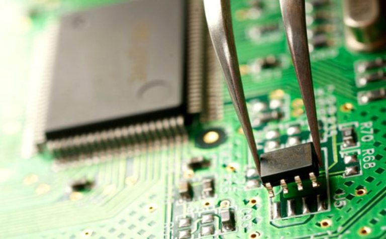
Gold Finger Plating and Beveling for Edge Connectors
Gold fingers are the part of a board that a mating connector grips, slides against, and wears every time the product is inserted. They are also one of the few features whose specification combines plating, geometry, and mechanical finishing in a single requirement. Getting the gold thickness right but the bevel wrong produces a card that damages its own contacts on the second insertion.
What Gold Fingers Do
A gold finger is an edge contact that transfers power or signal to a mating socket. It must conduct reliably, resist corrosion, and survive repeated insertion without losing its surface. Gold serves that purpose because it resists oxidation and keeps contact resistance low even after long storage, which is why it is used where the interface must work on the first attempt.
The finger is more than a plated strip. Its width, pitch, and length are set by the connector it mates with, and its thickness and finish determine how long the interface will last. The board edge beneath the fingers must also be shaped so that it enters the socket without scraping, which is where beveling enters the specification.
Hard Gold, Soft Gold and ENIG Compared
Hard gold is an alloy of gold with a small amount of cobalt or nickel, deposited electrolytically. The alloy raises hardness substantially, which is what makes it suitable for a sliding contact. Soft gold is purer and softer, offering the best conductivity and wire-bond compatibility but poor wear resistance, so it is used for bonding rather than for edge contacts.
Electroless nickel immersion gold is a different process entirely. It provides a thin, uniform gold layer over nickel without the need for a plating bus, and it protects pads well against corrosion. It is not, however, a wear surface, because the gold is only a fraction of a micrometre thick and is consumed quickly by abrasion.
The Nickel Underplate and Its Role
Gold is always deposited over a nickel barrier. The nickel provides hardness and mechanical support for the thin gold layer, and it prevents copper from diffusing into the gold, which would raise contact resistance and cause corrosion at the surface. A nickel layer that is too thin allows diffusion, while one that is too thick can crack during bending.
Typical specifications call for a few micrometres of nickel, with the exact range set by the connector and the application. The nickel also affects the appearance of the final surface; a dark or discoloured underplate usually indicates a plating chemistry problem rather than a gold thickness issue, and the two should not be confused.

Plating Process Control and Thickness
Electrolytic gold plating requires a conductive path to every finger, so the board needs a plating bus that connects them and is later removed. Current distribution across that bus determines thickness uniformity, and fingers at the far end of a long bus tend to plate thinner than those near the contact point. Racking design and current density therefore matter as much as bath chemistry.
Thickness is verified by X-ray fluorescence on the finished feature, since the gold layer is usually thinner than a micrometre for soft gold and a few tenths of a micrometre for hard gold on some specifications. Because measurement is quick, thickness data can be collected from several fingers per panel and trended, which is far more informative than a single certificate value.
Selective Plating, Masking and Taping
Gold is expensive, so it is applied selectively. The rest of the board is masked with tape, resist, or a plating mask, and only the fingers are exposed to the gold bath. Masking must seal tightly, because seepage produces gold on areas that cannot be soldered and must later be removed, which risks damaging the mask and the laminate.
The plating bus is removed after gold deposition by routing or etching, and the cut must not expose copper at the finger edge. When the bus is routed away, the cut line should be far enough from the connector contact zone to remain outside the mating envelope. Documenting that distance prevents a subtle incompatibility with the socket.
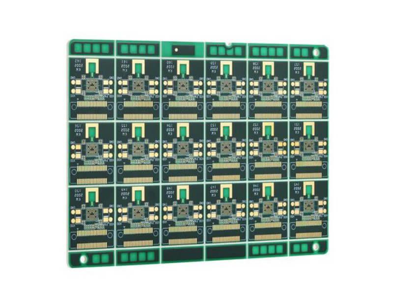
Beveling Angles and Edge Geometry
Beveling removes material from the leading edge of the board so the finger slides into the socket smoothly. A typical chamfer is around 30 degrees on each side of the board, though the exact angle and depth depend on the connector. Too shallow an angle leaves a sharp corner that scrapes the socket contacts; too deep a bevel cuts into the finger and reduces the contact area.
The bevel is produced by routing or by a dedicated beveling machine, and its depth is normally stated as a distance from the board edge along the surface. Where the connector has a low insertion force, a smaller chamfer may be acceptable, but the geometry should still be specified rather than left to the operator’s judgement.
Chamfer Quality and Inspection
Inspection checks the angle, the depth, and the condition of the cut. A ragged or chipped edge indicates a worn tool or an incorrect feed rate, and it will damage the socket if it is not corrected. Burrs, slivers, and exposed laminate at the bevel are common findings that a visual check under magnification will reveal.
The gold surface also needs checking after beveling, because the cut can lift or smear plating near the edge. Some specifications allow minor edge smearing outside the contact zone, while others require clean plating throughout. A dimensional check with a gauge or an optical comparator confirms whether the chamfer matches the drawing.
Wear, Insertion Cycles and Reliability
Wear life is usually expressed as a number of insertion cycles. A hard gold surface with adequate nickel underplate can withstand hundreds or thousands of cycles, depending on the contact force and the cleanliness of the mating socket. Soft gold on the same geometry may fail far sooner because the surface is simply removed.
Contact resistance is monitored during qualification, with samples cycled and measured at intervals. A rising resistance indicates that the gold has worn through, exposing nickel or the diffusion layer beneath. Because wear is accelerated by dust and by a poorly aligned socket, the test should use a representative connector rather than a laboratory fixture alone.
Design Rules and Documentation
The drawing should state the gold type, the thickness of gold and nickel, the bevel angle and depth, and the extent of the plated area from the board edge. It should also define the plating bus and how it will be removed, since that decision affects both the electrical test strategy and the final edge geometry.
Fabrication notes cover the rest: the finish on the remaining pads, the masking material, and the inspection criteria for the chamfer. When those details are missing, each supplier interprets them differently, and the resulting boards may work in one socket and fail in another for reasons that are difficult to diagnose after the fact.
FAQ
How thick should gold be on a gold finger? Hard gold for edge connectors is commonly specified between 0.5 and 1.5 micrometres over a nickel layer of several micrometres, with the exact value set by the required insertion cycles. Higher wear resistance comes from hardness and the nickel underplate rather than from gold thickness alone.
Can ENIG be used on gold fingers? It can be plated, but it is a poor choice for a sliding contact because the gold layer is extremely thin and wears through quickly. ENIG suits solderable pads and fine-pitch components; edge connectors that mate repeatedly should use hard gold.
Why does the bevel angle matter so much? The bevel controls how the card enters the socket. An angle that is too shallow leaves a sharp edge that scrapes the contacts, while one that is too deep reduces the contacting area of the finger. Specifying the angle and depth on the drawing keeps the finished geometry compatible with the connector.