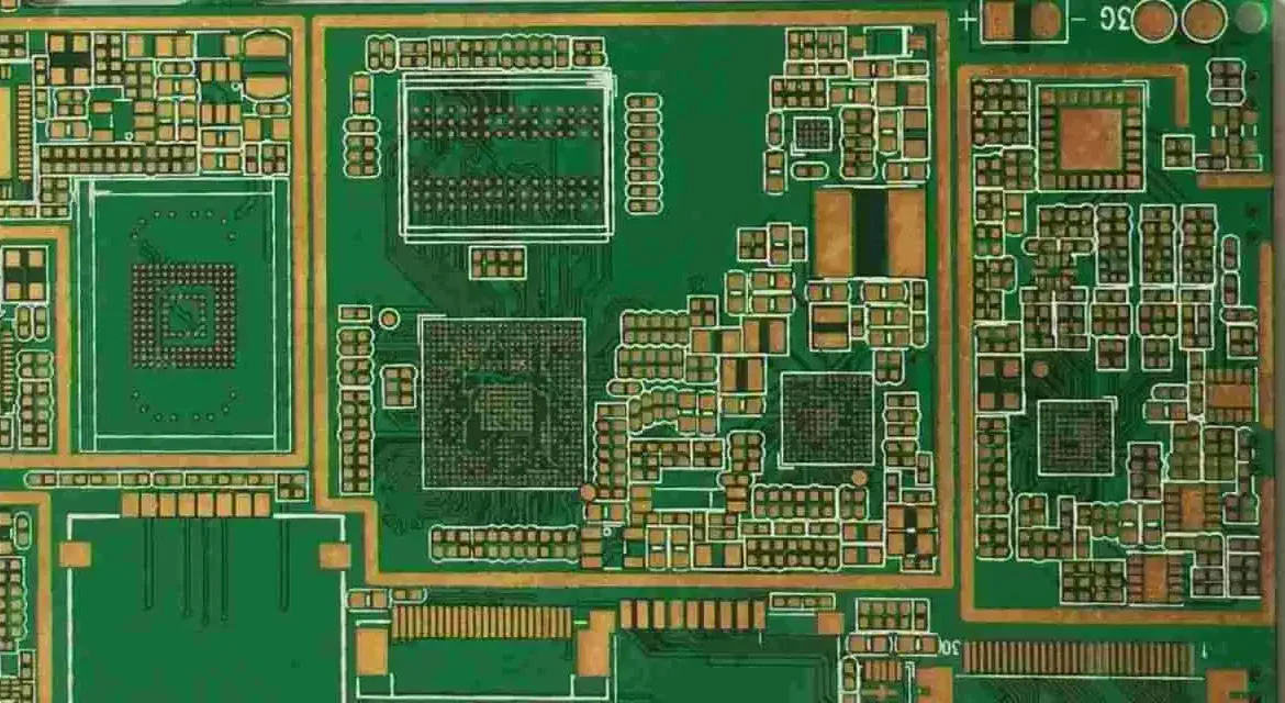
Copper Thickening In DPC Ceramic Substrates
Direct plated copper substrates begin as a thin sputtered seed layer on a ceramic surface, which is enough to carry a circuit but not enough to carry tens of amperes. Thickening that layer by electroplating is what turns the process into one suitable for power electronics, and it is also where most of the process difficulty lies.
This article describes why thickening is needed, what happens during the plating step, and the defects that appear when the process is not controlled.
The subject is a good example of a fabrication process whose limits are set by chemistry and by geometry at the same time, and where the parameters interact rather than acting independently.
Why Thin Copper Is Not Enough
A sputtered seed layer is measured in fractions of a micrometre. It carries signal currents adequately and it has excellent adhesion because the deposition is a physical process that forms a continuous interface with the ceramic. Its cross section, however, cannot carry a power current without an unacceptable temperature rise, and its thermal spreading capability is negligible.
Copper thickening adds metal by electroplating until the layer is tens of micrometres thick, which reduces the resistance proportionally and increases the cross section available for spreading heat. The trade is that the plated copper grows on a seed layer that must remain continuous and conductive, and the plating process has to be controlled to produce a uniform and adherent deposit. The ceramic substrate construction determines how much copper is practical.

How The Plating Step Works
The substrate is patterned with a resist, connected to a cathode and immersed in a copper sulphate bath. Current flows through the seed layer and copper deposits from the solution onto the exposed areas. The deposition rate depends on the current density, the concentration of the bath and the agitation, and it is inherently less uniform on a patterned surface than on a flat one.
Current crowds at the edges of features and at the corners of the pattern, so those areas plate faster than the centres of large pads. The result is a copper layer that is thicker at the edges and thinner in the middle, which is why the design of the pattern is part of the plating problem and why the plating additives that control the deposit distribution are critical to the process.
The Defects That Appear
Three defects dominate. The first is a non uniform thickness, which produces a component that behaves differently from its neighbours and which can create a step that resists the die attach. The second is a poor bond at the seed layer interface, which appears later as a delamination of the plated copper from the ceramic.
The third is a defect within the copper: a nodule, a pit or a void, each of which raises the local resistance and creates a place where a crack can begin. Brightening and levelling additives reduce all three, and the prevention of copper plating defects is largely a matter of keeping the bath chemistry within its window.
Process Control
The parameters that have to be controlled are the copper concentration, the acid content, the chloride level, the additive concentrations and the temperature. The additives are consumed during plating and are replenished by analysis rather than by volume, which is why a bath has a finite capacity expressed in ampere hours rather than in litres.
The agitation matters as much as the chemistry, because a depleted boundary layer at the surface produces a rough or powdery deposit. Agitation by movement, by air sparging or by a combination is chosen according to the aspect ratio of the features to be plated.
The thickness that a design requires should come from the current and the allowed temperature rise rather than from a habit. A conductor carrying a given current dissipates power in proportion to its resistance, and the resistance falls with the cross section. On a substrate that is also the thermal path, the same copper that carries the current spreads the heat, so the two requirements usually point in the same direction.
Thickness And Stress
Plated copper has internal stress, and the stress rises with thickness. On a rigid ceramic substrate the stress cannot be relieved by the substrate bending, so it appears at the interface with the ceramic and at the boundaries of the plated areas. A deposit with high tensile stress tends to crack; one with high compressive stress can lift the resist or buckle.
Stress is controlled through the additive system and through the current waveform. Pulse plating, in which the current is switched on and off, allows the concentration at the surface to recover during the off period and produces a denser deposit with lower stress than direct current plating at the same average rate.
Why The Pattern Matters
The pattern determines the current distribution, and therefore the thickness distribution. Isolated small features plate uniformly because the current has nowhere to concentrate. Large areas plate unevenly. Features connected to the plating bus by a thin neck may experience a voltage drop that reduces the current and the thickness.
The design responses are to balance the copper area across the panel, to provide adequate bus connections to each area, and where possible to use a pattern that avoids extremes of feature size on the same substrate. These are the same principles that apply to electroplating in general, applied on a substrate where the deposit cannot be corrected later by planarisation.
Where the pattern includes both power and control circuits, the difference in required thickness becomes a problem. The control features need resolution, which favours a thin deposit, while the power features need cross section, which favours a thick one. A common solution is to plate in two stages, with the fine features defined after the coarse ones, though this adds process steps and cost.
Verification
Thickness is measured by eddy current on the finished part or by cross section on a sample. Adhesion is measured by a peel test or by a thermal shock followed by inspection for delamination. Both tests should be performed on a coupon that has been processed with the production parts, because the plating behaviour depends on the panel and on the position within the bath.
The electrical consequence should also be confirmed: a measurement of the resistance of the conductor pattern on a known geometry gives an effective resistivity, which will be higher than the value for pure copper if the deposit is porous or contaminated. That measurement is a sensitive indicator of bath condition.
Finally, consider the interface between the plated copper and whatever is attached to it. A die attach or a wire bond is made to the top surface of the deposit, so that surface finish and its freedom from contamination matter as much as the thickness. A surface that has been exposed to the plating bath for a long time may carry organic residues that interfere with the joint.
FAQ
How thick can the copper be plated on a DPC substrate? The limit is the stress and the pattern resolution rather than the process itself. Beyond a certain thickness the features spread laterally and the resolution degrades, so the practical limit is set by the finest feature in the design.
Can the plated copper be machined flat afterwards? It can be planarised, but the process adds cost and risks damaging the surface. It is used where flatness is critical, as under a large die attached by sintering.
Does the seed layer affect the final conductivity? It contributes a small series resistance and, more importantly, its quality determines the adhesion and the uniformity of everything plated above it.