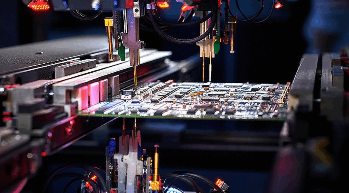
Copper Plating Defects in PCB Fabrication
Acid copper electroplating occupies a central place in board fabrication. The quality of the copper plating determines the quality and the mechanical properties of the copper layer, and it propagates into everything that follows, which is why controlling it is one of the harder process steps even for large manufacturers. The defects that recur are few and well known: rough deposits, particles on the surface, pits, and whitening or uneven colour. Each has a set of causes that can be narrowed down systematically.
Rough Plating
The most common form is roughness concentrated at the corners of the panel, and the usual cause is plating current that is too high. Reduce the current and verify the reading with a clamp meter to make sure the displayed value is real.
Roughness across the whole panel is unusual, but it does happen. In one case the cause turned out to be a combination of low ambient temperature in winter and insufficient brightener content in the bath. Boards that have been through rework and resist stripping with an incompletely cleaned surface can also show the same symptom, which is a reminder that roughness is not always a plating defect.
Copper Particles on the Surface
Particles can originate anywhere along the chain — in the electroless copper line, in pattern transfer, or in the plating bath itself.
From the electroless copper process. Almost any step in the sequence can be responsible.
Alkaline degreasing in hard water, combined with heavy drilling dust — particularly on double-sided boards that skip desmear — and inadequate filtration, produces roughness on the hole walls and sometimes on the surface. Light point contamination on the surface can usually be removed by micro-etching.
Micro-etching contributes its own set of failures. Hydrogen peroxide or sulfuric acid of poor quality, or ammonium persulfate with too high an impurity content, causes trouble; the recommendation is to use at least chemically pure grade, since industrial grade introduces additional quality failures beyond this one. A micro-etch bath with excessive copper content, or one running at low temperature, allows copper sulfate to crystallise out slowly. A cloudy, contaminated bath is another source.
The activation bath is frequently at fault. Contamination or poor maintenance — a leaking filter pump, specific gravity that is too low, copper content that is too high because the bath has been in use for more than three years — generates particulate suspension or colloidal impurities that adsorb onto the surface and the hole walls, usually accompanied by roughness inside the holes. Accelerator or desmear baths used beyond their life also turn turbid; because most are formulated with fluoroboric acid, they attack the glass fibre in FR-4, raising the silicate and calcium content of the bath, and increases in copper and dissolved tin content produce the same particle problem.
The electroless copper bath itself contributes when its activity is too strong, when the air agitation carries dust, or when solid fines are suspended in the solution. Adjusting the process parameters, replacing or adding air filter elements, and filtering the whole bath are the standard remedies.
The dilute acid tank used to hold boards after electroless copper also matters: it has to stay clean and be replaced when it turns cloudy. And boards should not be stored too long after the electroless step, because the surface oxidises even in acid solution, and an oxide film is harder to remove than the original contamination.
One diagnostic detail is useful. Particles originating in the electroless line, other than those from surface oxidation, tend to be distributed fairly evenly and follow a recognisable pattern. Whether the contamination is conductive or not, it will produce particles in the plating that follows. Test panels can be processed step by step for comparison, and boards with the fault in production can often be corrected by gentle brushing with a soft brush.
From pattern transfer. Residual resist after development is a cause — even an extremely thin film can be plated over and encapsulated by the copper, which is why development is checked rather than assumed, as described in this discussion of photoresist developing control. Incomplete rinsing after development does the same thing, and so does storing boards too long after imaging, which allows the surface to oxidise, particularly when rinsing has been poor or the workshop air is heavily contaminated. The remedies are straightforward: strengthen rinsing, schedule the work so that boards move through promptly, and increase acid degreasing strength.
From the plating bath itself. Failures here fall into four groups.
Parameters: sulfuric acid content too high, copper content too low, or bath temperature too low or too high. A plant without temperature control is particularly exposed, because the usable current density window narrows, and operating at normal production settings then generates copper powder inside the bath which mixes into the solution.
Operation: plating current too high, poor clamping, dry contact points, or boards that have dropped into the tank and dissolved near the anode. All of these concentrate current on part of the load and produce copper powder, which then settles and gradually becomes a particle defect.
Materials: the phosphorus content of the phosphor copper anode and the uniformity of its distribution.
Maintenance: the periodic treatment of copper balls, and cleaning of the anodes and anode bags, which many plants perform poorly. Copper balls should be cleaned and micro-etched with hydrogen peroxide to expose fresh copper, and anode bags should be soaked in sulfuric acid and hydrogen peroxide, then in alkali, and rinsed thoroughly. Anode bags should use polypropylene filter material with a pore size of five to ten micrometres.
Plating Pits
Pits can arise at several stages, from electroless copper through pattern transfer, pre-treatment, copper plating and tin plating.
From electroless copper. Plating baskets that are not cleaned properly retain contaminated solution containing palladium and copper, which drips onto the board surface during micro-etching and creates localised contamination. After plating this appears as spot voids, which is to say pits.
From pattern transfer. The causes are mostly equipment maintenance and incomplete development or rinsing: contaminated brush or squeegee rollers and water-absorbing rollers carrying adhesive residue, air knives and blowers with oil or dust inside, inadequate dust removal before lamination or printing, incomplete development, poor rinsing after development, and contamination of the surface by silicone-based antifoam agents.
From pre-treatment. Acid degreasing, micro-etching and pre-dip all contain sulfuric acid as a principal component, so hard water produces turbidity and contaminates the surface. Rack coatings that dissolve into the bath over time contaminate the solution as well. In each case, non-conductive particles adsorb on the board and produce pits of varying severity in the plating that follows.
From the plating bath. Air agitation that is uneven because the sparge pipes have shifted from their position; a leaking filter pump, or an inlet located close to the sparge pipe, drawing in air and generating fine bubbles that adhere to the board surface or along the edges of traces, particularly on horizontal trace edges and at trace corners. A further cause is low-quality filter cores that were not fully processed: antistatic agents used during their manufacture contaminate the bath and cause plating voids. Increasing air agitation and clearing foam from the surface promptly addresses this, and filter cores should be soaked in acid and alkali before use.

Whitening and Uneven Colour
Surface colour defects are usually a brightener or maintenance problem, and occasionally a rinsing or micro-etch issue.
Imbalance of the brightener system, severe organic contamination, and bath temperature that is too high all produce it. Acid degreasing normally does not create a rinsing problem, but if the water supply is acidic and carries a high organic load — recycled rinse water is the usual case — rinsing can be inadequate and the micro-etch becomes uneven. On the micro-etch side, low etchant content, high copper content in the solution and low bath temperature all produce uneven results.
There is also a sequencing effect. Poor rinse water quality, a slightly longer rinse time, or contamination of the pre-dip acid can leave a light oxide on the board. Because the entry into the copper bath is on load and the oxide is acidic, it is difficult to remove, and the result is an uneven colour. Boards touching the anode bag, uneven conduction through the anode, and anode passivation produce the same defect.
Where to Look First
Three habits shorten the diagnostic path.
Use small test panels processed step by step, so that a fault can be attributed to the electroless line, to imaging or to plating rather than being guessed at. For boards already affected in production, gentle brushing with a soft brush resolves the surface particle cases without scrapping the panel.
Treat consumables as process variables. Filter cores, anode bags and air filters all interact with the chemistry, and cheap or unprocessed versions introduce contamination that no parameter adjustment will compensate for. The same principle applies to the chemistry itself: chemical grade of micro-etch reagents is not a place to economise.
Finally, keep the whole plating chain in view. A defect that appears in the plating bath is frequently created three steps earlier, and the same is true of the defects that reach customers, as described in this overview of PCB inspection after fabrication. The metallisation that precedes plating is a particular candidate, and the alternatives available there are described in this note on the black hole process and electroless copper.
FAQ
Why does roughness appear mainly at the panel corners? Because current density is highest there. Reducing the plating current and confirming the reading with a clamp meter resolves the majority of corner roughness cases.
What causes particles that form inside the holes? Alkaline degreasing in hard water combined with heavy drilling dust and poor filtration is the classic cause. It roughs the hole wall as well as the surface, and the surface portion can sometimes be removed by micro-etching.
Why does the anode bag material matter so much? Because the bag is a filter in the current path. A polypropylene bag with five to ten micrometre pores, cleaned properly before use, keeps anode sludge out of the plating; a poor one releases contamination into the bath.