PCB Handling Damage and Scratch Prevention in Assembly
Most boards are damaged before they are tested. A panel dragged across a bench edge, a stack slid without interleaving, or a connector dropped onto a rail leaves marks that may be cosmetic, may be repairable, or may have broken a trace the operator cannot see. Handling damage is the least technical defect in electronics and often the hardest to eliminate.
What Handling Damage Looks Like
Handling damage covers scratches through the solder mask, nicks on the board edge, chipped laminate, bent connector pins, cracked components, and contamination transferred from fingers or packaging. Some of it is visible immediately, while other damage, such as a lifted pad or a hairline crack in a ceramic capacitor, appears only after thermal stress.
Severity depends on location and depth. A scratch on a ground pour with mask over it is usually cosmetic, while the same mark across a signal trace in a high-impedance node damages the impedance and may break the conductor. Cosmetic and functional criteria must therefore be defined separately in the acceptance specification.
Where Damage Happens in the Process
The process contains many transfer points: bare board receipt, drilling and routing, plating racks, assembly loading, conveyor transfer, test fixtures, depanelling, and packing. Each transition is an opportunity for a board to contact a hard surface or to be gripped too tightly. The most common single location is wherever boards are stacked and moved by hand.
Unpacking and packing are frequently overlooked. Slide a board out of a tight carton and its edge grinds against the cardboard and any debris inside. Stack bare boards without interleaving and the copper on one board contacts the mask on the next, leaving marks that appear after lamination or assembly. Cardboard dust and tape residue are equally common and show up later as poor adhesion in a coating or a printing step.
Panel Handling and Conveyor Effects
Panels are heavier than they look, and the edges that the conveyor grips are the most exposed part of the assembly. Rails set too tight scratch the mask; rails set too loose allow the panel to skew and touch a guide. Worn conveyor components mark the board edge consistently, which produces a pattern that is easy to identify once someone looks for it.
Board supports and stop positions also cause damage. A misadjusted stop can drive a panel into a hard gate, and a lifting pin that misses its target can push through the laminate. Machine adjustments should be verified after any maintenance or product change, because a small shift in a stop position is invisible until boards arrive at inspection with matching marks. A weekly walk along the board path, from station to station, finds more of these issues than any amount of defect analysis.

Gloves, Tools and Workstation Practice
Bare hands transfer oils and salts that accelerate corrosion and interfere with soldering, so gloves are standard in most assembly areas. The glove material matters: nitrile is common, while latex and some vinyl formulations leave residues. Gloves also need changing, because a contaminated glove spreads as much as a bare hand.
Tools cause damage when they are used for the wrong purpose. Metal tweezers scratch mask, screwdrivers slip, and cutting tools leave burrs. Providing the correct tool for each task, keeping work surfaces clean, and giving each board a defined place to rest removes most of the opportunity for accidental contact.
Mask Nicks, Scratches and Cosmetic Criteria
Cosmetic criteria define how much mask damage is acceptable and where. Typical rules address the size and depth of a scratch, the number permitted per panel, and the area within which no damage is allowed, such as over a connector footprint or a gold finger. Without written criteria, the decision becomes a matter of opinion at inspection.
The criteria should also state what is explicitly prohibited. Exposed copper on a conductor, damage that reduces the width of a trace, and any mark within a mating surface are normally rejectable regardless of size. Photographs of borderline examples remove much of the ambiguity and speed up training.
Repairing Mask Damage Acceptably
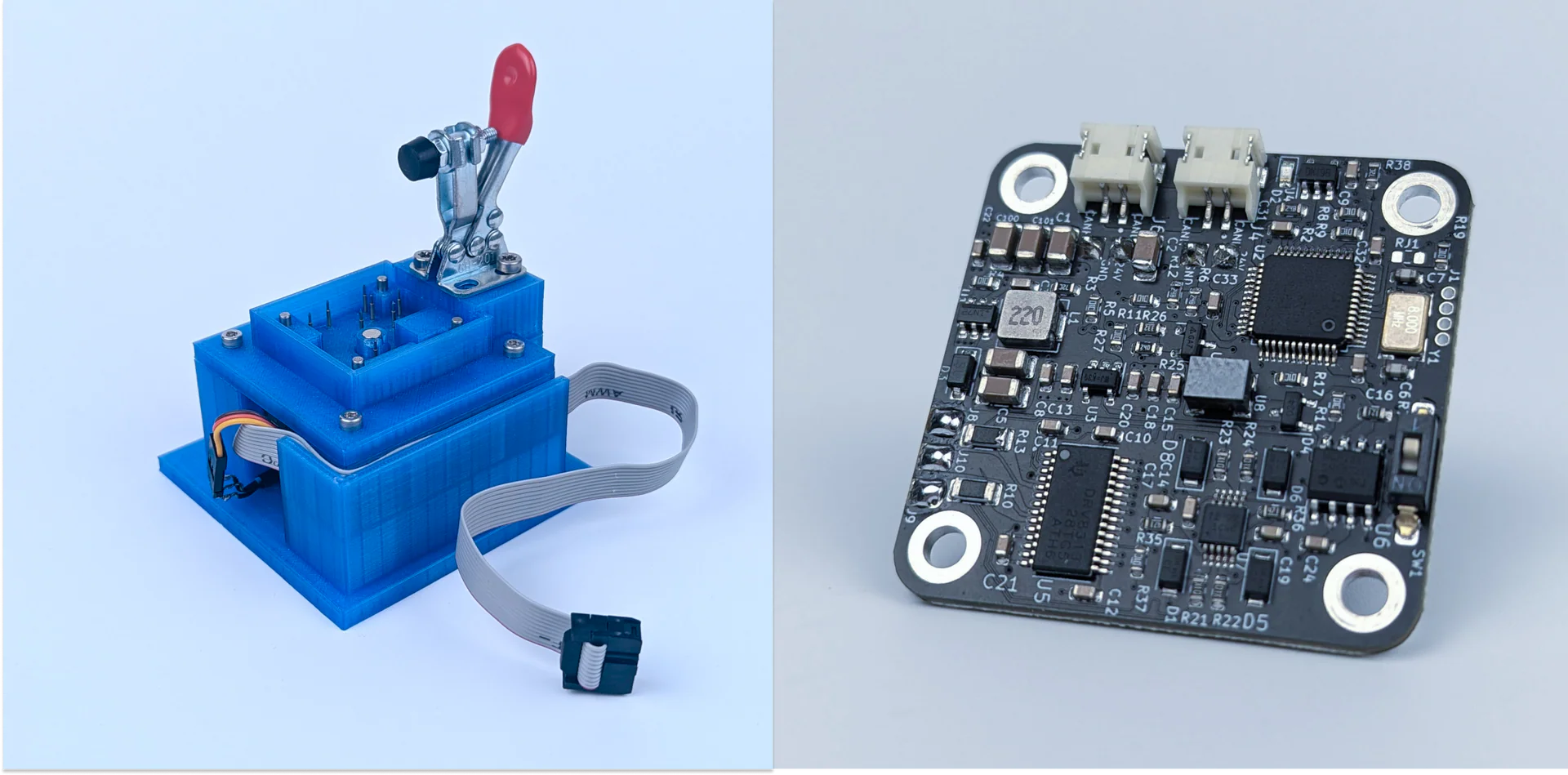
Solder mask damage can sometimes be repaired with a compatible mask ink that is cured in place. The repair must restore dielectric strength and adhesion, and it must survive the thermal cycles the assembly will see. Where the damage exposes a conductor, the repair also has to protect against corrosion and electrochemical migration.
Repair is not always the right answer. Damage over a fine-pitch area, damage that has disturbed the copper, and damage on a high-reliability product may justify scrap. The decision rule should be written, with the maximum repair size and the products on which repair is permitted stated in advance. Where repair is allowed, the operator should record the location and the material used, because a repaired area behaves differently under thermal cycling.
Packaging, Stacking and Transport
Packaging protects the board between processes as well as between the factory and the customer. Interleaving sheets, edge protectors, and rigid cartons prevent board-to-board and board-to-wall contact. Boxes should be filled so that the contents cannot shift, because movement during transport converts a well-packed stack into a grinding one.
Stacking limits deserve attention too. Excessive weight deforms the lower boards and presses their features into the one below, and stacked assemblies with tall components can damage each other. Where parts are fragile, a tray or a rack is better than a stack, even though it takes more space.
Inspection, Records and Feedback
Handling damage is best controlled by looking for patterns. Damage that appears in the same position on many boards points to a machine or a fixture, damage concentrated at one station points to a method, and random damage usually points to a handling habit. Recording location and type turns scattered findings into a diagnosis.
Photographs of each defect type should be shared with the stations involved rather than filed with quality. People correct what they can see, and a picture of a specific scratch pattern on the conveyor rail is far more persuasive than a defect rate quoted in a meeting.
Training and Prevention Culture
Training should explain the consequence, not only the rule. An operator who understands that a scratch can change the impedance of a trace handles boards differently from one who has been told to be careful. Short, regular sessions with real examples work better than a single induction course.
Prevention also relies on the environment. Clean, uncluttered benches, adequate lighting, defined storage locations, and enough time in the cycle to handle panels properly all reduce damage. Where a process is so rushed that boards are thrown into a bin, no amount of training will hold. Supervisors set the pace, and a station given unrealistic cycle times will invent shortcuts whether or not anyone asks for them.
FAQ
Is a scratch on the solder mask always a defect? No. A light mark over an unconnected area is usually cosmetic, while damage that exposes copper, crosses a trace, or sits within a mating surface is normally rejectable. The criteria should define size, depth, location, and the number of marks permitted per board.
Can damaged solder mask be repaired? Yes, within limits. A compatible ink cured in place can restore protection if the damage is small and the conductor beneath is intact. Damage over fine-pitch features, or any damage that has disturbed the copper, is usually a scrap decision.
What is the most common source of handling damage? Manual transfers, particularly moving stacked boards between stations. Automatic handling removes most of it, but where boards are still moved by hand, interleaving, correct stacking limits, and gloved handling eliminate the majority of marks.