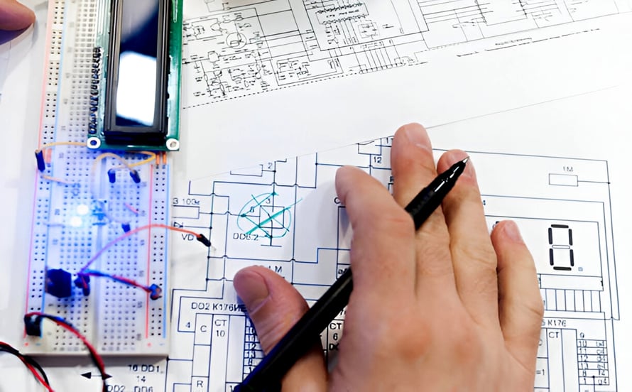
Return Via: Via Design for High Speed Channels
Vias are the cheapest way to connect layers and the most expensive way to ruin a high speed channel, because the same feature that provides the connection also introduces a discontinuity. Designing them deliberately rather than by default is what separates a working channel from a marginal one.
The Two Electrical Effects of a Via
A via presents capacitance to every plane it passes and inductance along its barrel. The capacitance comes from the pad and the copper around it, and the inductance from the length of the barrel and the area of the return loop.
At low frequency both are negligible, and at high frequency both matter. The capacitance reduces the impedance at the via, while the inductance raises it, and the net effect depends on which dominates for the geometry in question. Our signal integrity notes describe the analysis.
Reducing the Capacitance
The capacitance is proportional to the pad diameter and to the antipad, which is the clearance in the plane. Reducing either reduces the capacitance, and both are constrained by the drill tolerance and by the electrical clearance requirement.
Removing the pad entirely on the layers where the via does not connect is a standard technique and it reduces the capacitance substantially. The practice is known as a non-functional pad removal and it should be specified rather than left to the shop. Our HDI via notes describe the related processes.
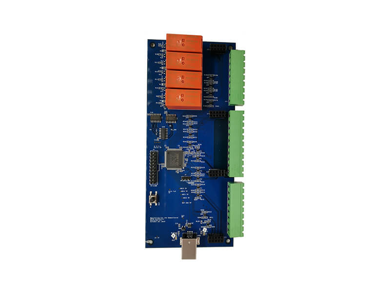
Return Vias and the Ground Path
The inductance of a via depends on the return path as much as on the barrel, because the loop energy is stored between them. A ground via placed adjacent to the signal via gives the return a short path and reduces the loop.
The distance between the two determines the benefit, and the vias should be placed on the same pitch as the trace’s reference rather than at a convenient location. The return via is particularly important at a layer change, where the reference plane itself changes.
Stub Length and Resonance
Where a via passes through the board and the signal uses only part of it, the remainder is a stub. The stub behaves as a transmission line with a short circuit at the far end, and it resonates at the frequency where its length is a quarter wavelength.
Below that frequency the stub adds a small amount of loss, and above it the channel has a notch. The remedy is a shorter barrel, achieved by a thinner board or a blind via, or a backdrill that removes the stub after plating.
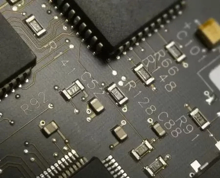
Via in Pad and the Soldering Problem
A via inside a solder pad has to be filled and capped, or the solder wicks into the barrel and leaves a void in the joint. The fill is an additional process and it should be specified in the data.
The alternative is to move the via outside the pad and connect it with a short trace, which costs routing area but avoids the fill. The trade is decided by the device pitch and by the number of vias in the pad area.
Choosing a Via Geometry
The geometry follows from the requirement: a small via with a short barrel for a fast signal, a larger via with a thicker barrel for a power connection, and an array of vias for a thermal path. Using one geometry everywhere compromises all three.
A small library of via types is easier to check than a design with a different via for every net, and the design rule check becomes meaningful when the types are few.
Simulating and Measuring
The via can be included in a channel simulation, and the modelling requires the geometry and the material properties rather than the net name. Where a simulation is not available, the experimental approach is to measure the channel with and without the via and to compare the eye diagrams.
The measurement is made on a coupon that carries the same via geometry as the product, so that the result describes the design rather than a test structure. Our test coupon notes describe the patterns.
Documenting the Requirement
The drawing should state which vias are to have their non-functional pads removed, which are to be backdrilled and to what depth, and which are to be filled. Those are process instructions that cannot be inferred from the artwork.
Where a backdrill depth is specified, the tolerance on the board thickness has to be considered, because the depth is measured from the surface and the surface moves. The two together determine whether the stub is removed and whether the barrel is damaged.
Process Control and Verification
On a design of this kind, non-functional pad is the item that decides how the rest of the board is arranged. Documenting the assumption is part of the design work, and a short note on the drawing prevents a question that would otherwise arrive a day later and cost a day of schedule. The process window is set by the narrowest step in the flow, so an improvement anywhere else shows up as margin rather than as yield until that step is addressed.
A short note on the drawing about handling, storage or packaging is often worth more than an extra decimal place on a tolerance. Where a value sits close to a process limit, the drawing should say so, since the shop can then open the process window rather than working to a nominal figure that carries no tolerance.
A stack-up that is drawn rather than described removes most of the ambiguity from a quotation, and it lets the fabricator price the board against the dielectric and copper weights that will actually be used.
Process Control and Verification
On a design of this kind, non-functional pad is the item that decides how the rest of the board is arranged. Documenting the assumption is part of the design work, and a short note on the drawing prevents a question that would otherwise arrive a day later and cost a day of schedule. The process window is set by the narrowest step in the flow, so an improvement anywhere else shows up as margin rather than as yield until that step is addressed.
A short note on the drawing about handling, storage or packaging is often worth more than an extra decimal place on a tolerance.
Process Control and Verification
On a design of this kind, non-functional pad is the item that decides how the rest of the board is arranged. Documenting the assumption is part of the design work, and a short note on the drawing prevents a question that would otherwise arrive a day later and cost a day of schedule. The process window is set by the narrowest step in the flow, so an improvement anywhere else shows up as margin rather than as yield until that step is addressed.
FAQ
Do all high speed vias need ground vias? They need one wherever the reference plane changes, and they benefit from one wherever the via is a significant discontinuity. Where the channel is short and the frequency modest, the improvement is small.
How is stub length calculated? From the distance between the layer the signal uses and the far surface of the board, using the propagation velocity of the material. The resonant frequency is where that length equals a quarter wavelength.
What does gopcb confirm about via design? We confirm the via and pad diameters against our process, the aspect ratio, the antipad clearance, the non-functional pad removal, the fill requirement and the backdrill depth and tolerance. Where a combination is not producible at the quoted price we say so before the panel is released.