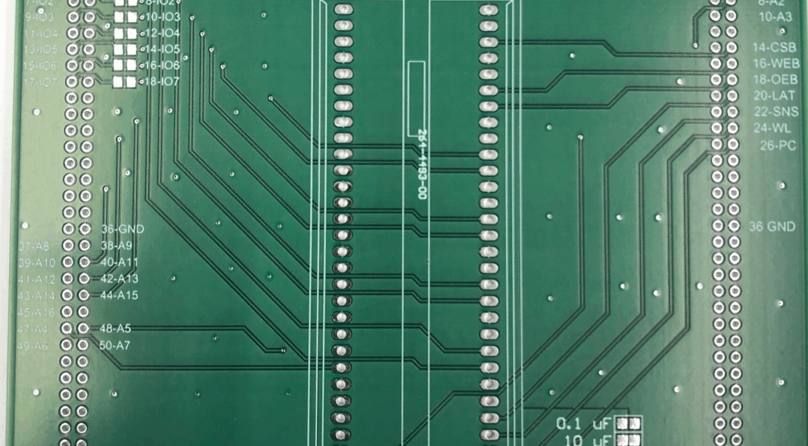
Incoming Inspection: Building a Program That Actually Works
Incoming inspection is the checkpoint where a delivered lot of printed circuit boards is judged against the order before it enters stores, and it is the last cheap moment to find a mistake. A bare board that looks perfect can carry a plating fault, the wrong laminate or a missing certificate, and none of those are visible from the outside of the package.
Why Incoming Inspection Exists
The purpose is not to repeat the fabricator testing, which would be wasteful, but to confirm that what arrived is what was ordered and that the evidence supporting it is complete. That covers the material grade, the finish, the stack-up, the dimensions, the electrical test data and the paperwork that ties them to a lot number.
A program built on that basis finds the errors that matter and ignores the ones that do not. Inspecting every board for cosmetic perfection, on the other hand, rejects good material and consumes the attention that should be spent on the features that actually predict field failure. On a mature programme the inspection plan is deliberately short, because every check added has to earn its place by catching something the process cannot be trusted to control.
Documentation and Traceability
The first check is administrative. The packing list, the certificate of conformance, the material declarations and the electrical test report should all name the same lot and the same part number, and the test data should be traceable to the panels that were actually shipped rather than to a generic file. A supplier that cannot produce the record is telling the customer something about how the boards were made, and that is a finding in itself.
The certificate also carries the promise that matters most: that the board was built to the revision and the specification on the purchase order. Where a supplier substitutes a laminate or a finish, the substitution is usually legal but it must be declared, and goods received without that declaration should not be accepted silently.

Visual and Dimensional Checks
Visual inspection looks for the defects that a bare board can carry: scratches through the mask, exposed copper, solder mask voids, discoloured finishes, edge damage from routing and contamination on the pads. Good lighting and a defined magnification matter more than the inspector, because most of these faults are contrast defects.
Dimensional checks confirm the outline, the hole sizes, the slot positions and the thickness against the drawing. The critical dimensions are the ones that the assembly process depends on, such as the position of tooling holes, the coplanarity of a press fit connector area, and the location of the fiducials that the placement machine will use. Where assembly runs on a panel fixture, the panel dimensions and the breakaway tab positions deserve the same level of attention.
Solderability and the Surface Finish
Solderability is a process property rather than a material property, and it can be lost during storage even when the finish was correct at the factory. A simple wetting check on a sample pad confirms that the finish is still active, and our solderability test guide describes the methods available.
Finish thickness matters as well. Immersion silver and OSP layers are thin by design and are consumed by a single reflow, while ENIG carries a gold layer whose thickness has to be sufficient to protect the nickel from oxidation without making the joint brittle. Both figures are normally declared on the certificate.
<img src="https://www.gopcba.com/wp-content/uploads/2026/08/hdi-pcb-design-guidelines-11-b6900f71.webp" alt="Microsection of a plated through hole under a microscope” />
Microsection and Plating Thickness
Destructive testing answers the questions that appearance cannot. A microsection shows the plating thickness in the hole, the copper to resin bond, the degree of etch and the presence of voids, cracks or resin smear, and a plating thickness report gives the numbers behind the picture.
Because the test destroys the sample, it is performed on a coupon or a spare board rather than on the deliverable. The coupon should come from the same panel and the same lot, and it should carry the same hole sizes and the same layer count as the product, otherwise the result describes a different board.
Electrical Test Evidence
Electrical test data should accompany the lot, whether it was produced by flying probe or by a fixture. The report identifies the net list that was tested, the continuity and isolation results, and the number of boards that failed and were repaired before delivery. Repairs are not automatically a problem, but an undocumented repair is, because it conceals a process that was out of control at the time it ran.
The net list revision is the part that is most often overlooked. A report showing that every net passed is worthless if it was generated from an older artwork revision, and our flying probe notes describe how the test programme is built from the design data.
Sampling Plan and Acceptance Criteria
A sampling plan turns inspecting into a decision with a defined risk. It states how many boards are drawn from the lot, which characteristics are measured on them, and what acceptance criteria apply, so that a lot is accepted or rejected on the same basis by any inspector and on any shift.
Critical characteristics such as the net list, the layer count and the finish should be verified on every board or against the panel records, while cosmetic features can reasonably be sampled. Mixing the two is the common mistake, because it either over-tests the trivial or under-tests the fatal.
Handling, Packaging and Storage
Bare boards are easily damaged once they leave the bag. Vacuum packing with a desiccant protects the finish from humidity, edge protection prevents rub marks during transport, and the bag should stay closed until the boards are actually required on the line.
Shelf life is counted from the packing date and depends on the finish. Boards held beyond it should be re-checked for solderability rather than used on trust, because a finish that has oxidised will produce poor joints that look like a solder paste problem on the assembly floor. Many solderability complaints are traced back to storage rather than to the fabricator.
Closing the Loop With the Supplier
Inspection only pays back if the findings travel. A rejected lot with a clear photograph, a measurement and the specification clause that was breached gives the supplier something to act on, and a pattern of findings over several lots is what justifies a change of material or process.
It is equally important to feed back the good news. Suppliers that receive consistent, well documented feedback develop a feel for what the customer cares about, which reduces the chance of a substitution and improves the accuracy of the quotes returned. Our judging PCB quality notes describe the same loop from the fabricator side.
FAQ
Should every incoming lot be microsectioned? No. Microsection is destructive and belongs to a sampling or qualification routine, or to a lot where the paperwork or the plating report raises a question that cannot be answered another way.
Who writes the acceptance criteria for bare boards? Usually the customer, with input from the fabricator. Referencing a published standard for the generic features and adding the specific dimensions from the drawing produces a document both sides can work to.
How does gopcb support incoming inspection? Each lot ships with a certificate of conformance, material declarations, a plating thickness report and electrical test data traceable to the lot, and we supply coupons or spares on request so the customer can verify without sacrificing product.