Thermal Vias Under Power Devices: Design and Verification
A power device on a board dissipates heat that must travel through the package, through the solder, into the copper and out to the air or to the chassis. A thermal via array is the route through the board, and its design is a matter of geometry rather than of guesswork.
The Path and Where the Resistance Sits
Thermal resistance is expressed as degrees per watt, and the contributions add along the path. The junction to case resistance is given by the device data sheet, the case to board resistance depends on the solder joint, and the board to ambient resistance depends on the copper and the airflow.
In a well designed assembly the junction to case and the board to ambient terms usually dominate, which is why adding vias to a design that already has enough copper produces less improvement than expected.
Where the board to ambient term is the largest, the answer is more copper area or more airflow rather than more vias. Where the case to board term is small and the board to ambient term is small, the vias become the limiting element.
What the Vias Contribute
A plated via filled with copper has a thermal conductivity far higher than the laminate it displaces, so a small number of vias can carry a substantial part of the heat through a board. The copper in the barrel is thin, however, and the barrel is not filled with copper in a standard process.
The effective cross section of a via is therefore much smaller than its drilled diameter suggests, which is why a single large via is not equivalent to a number of small ones with the same total drill area.
Vias placed directly under the thermal pad are the shortest path. Vias placed at the edge of the pad must first conduct laterally through the pad copper, which adds resistance.
Geometry That Works
A grid of small vias on a pitch that leaves enough copper between them is the usual arrangement. The pitch must respect the solderability requirement, since vias in the pad tend to wick solder away from the joint during reflow.
The classical remedy is to tent or plug the vias on the component side so that solder cannot escape, while leaving them open on the other side. Plugging with a filled via process is more expensive and gives a flat pad, which reduces voiding.
Where the vias are open, the solder loss can produce an insufficient joint on the very pad that needs a good thermal connection. Our plating thickness notes describe the copper available in the barrel that provides the thermal path.

Spreading on the Far Side
The vias deliver heat to a copper area on the opposite side, and that area must be large enough to dissipate it. A via array that terminates in a small pad simply moves the bottleneck.
The spreading area is usually a solid copper region connected to a plane, and its effectiveness depends on the copper thickness and on whether it faces moving air. Our current capacity notes describe how copper area is sized for both current and heat.
Where the board is mounted to a metal chassis, a thermal interface material between the copper area and the chassis can reduce the board to ambient term substantially, and it is often cheaper than adding copper.
Designing the Pad and the Stencil
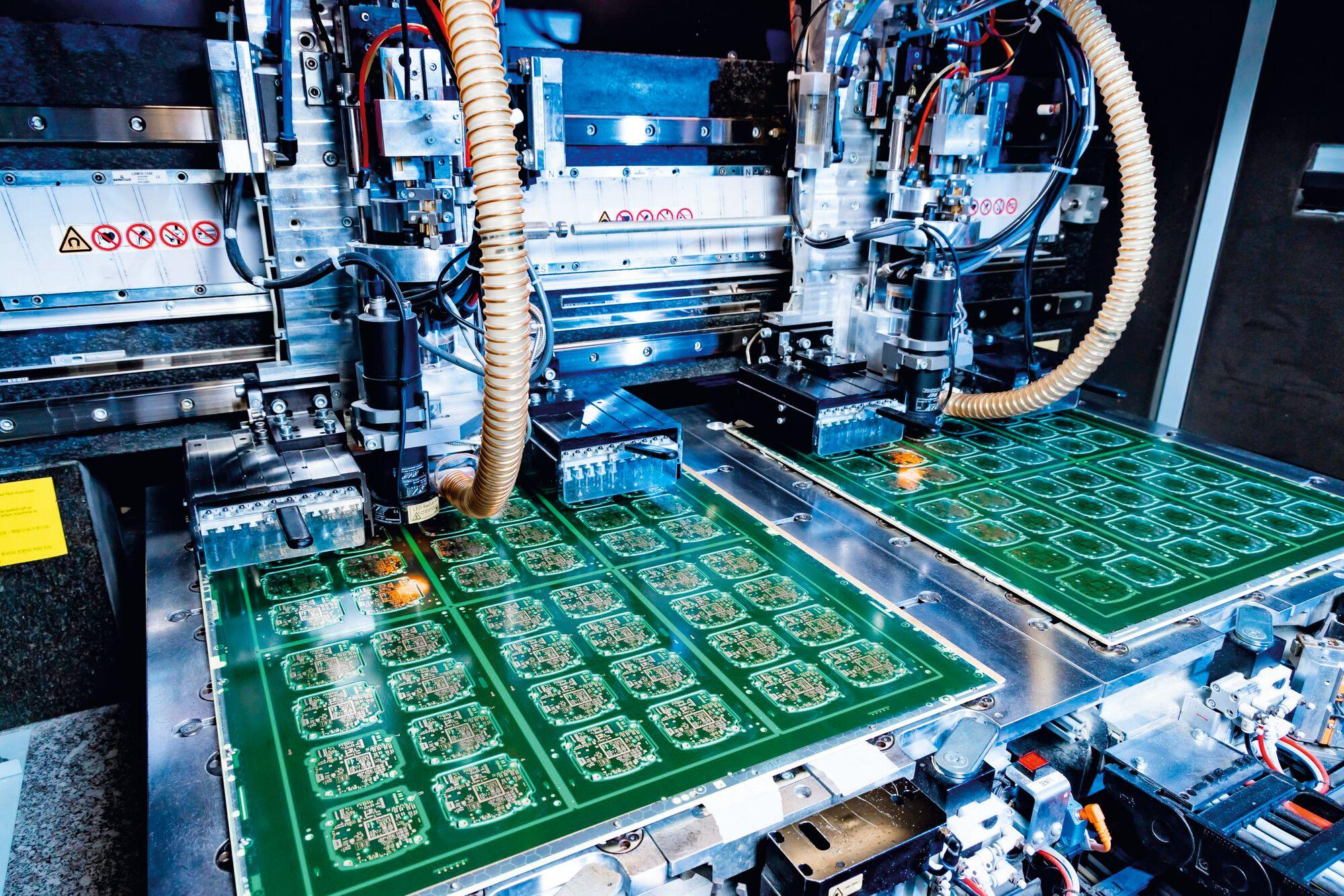
The thermal pad on the board is usually the same size as the device pad, and the stencil opening is divided into a grid to control the paste volume and reduce voiding. The division also provides channels for flux volatiles to escape.
A paste volume that is too high produces a thick joint with large voids and poor thermal contact. A volume that is too low produces an incomplete joint with gaps that are equally poor conductors.
The target is a joint that is thin, continuous and free of large voids, and the way to achieve it is to control the paste volume rather than to add more paste in the hope of better contact.
Verification
The first verification is the void content of the joint, measured by X-ray or by scanning acoustic microscopy. Acceptance criteria vary, but a large void under the centre of a thermal pad is the worst case because it sits directly in the thermal path.
The second is the actual temperature of the device in the assembled product, measured with a thermocouple on the case or by an infrared camera with the emissivity corrected. The measurement should be made at the worst case ambient and load, not at a convenient one.
Our thermal design notes describe the measurement setup and the way the result is compared against the junction limit.
When Vias Are the Wrong Answer
Where the device is mounted to a heatsink through the board, the thermal path is mechanical rather than electrical and the vias are irrelevant. The design then concentrates on the mechanical interface and on the flatness of the board.
Where the dissipation is small, a copper area on the component side may be sufficient, and the vias add cost without benefit. The calculation, not the habit, decides.
Where the board must be electrically isolated, thermal vias connected to a plane may create a capacitance that affects the switching behaviour of the device. Our switching regulator layout notes describe how the loop area and the copper areas interact.
Manufacturing Considerations
A dense via array under a large pad increases the local copper content, which changes the resin flow during lamination and can affect the thickness of the dielectric below. This matters most on thin boards and on impedance controlled layers nearby.
Vias that must be plugged add a process step, and the plugging material must be compatible with the surface finish and with the assembly process. A plugged via that is not fully cured can outgas during reflow.
Where the array is at the limit of the process, discussing it with the fabricator before the design is released is cheaper than discovering afterwards that the pitch cannot be drilled and plated reliably.
Additional Considerations for This Build
Practical attention to junction temperature pays for itself here, because it decides whether the finished board behaves as the drawing intended. Where the requirement is not stated on the fabrication drawing or in the assembly notes, the shop has to assume a default, and that default is rarely the value the design was simulated with. Stating junction temperature explicitly, together with the tolerance that applies, removes the assumption and keeps the result predictable from batch to batch.
Process Control and Verification
On a design of this kind, copper area is the item that decides how the rest of the board is arranged. Where a value sits close to a process limit, the drawing should say so, since the shop can then open the process window rather than working to a nominal figure that carries no tolerance. A stack-up that is drawn rather than described removes most of the ambiguity from a quotation, and it lets the fabricator price the board against the dielectric and copper weights that will actually be used.
FAQ
How many thermal vias are enough? Enough that the via array is not the dominant term in the thermal resistance calculation, which is a computation rather than a rule of thumb.
Should thermal vias be filled? Filling gives a flat pad and prevents solder loss, at the cost of an extra process step. Open vias are acceptable where the paste volume is controlled and light loss is tolerable.
What does gopcb provide for a thermal design? We provide via array layouts matched to the pitch and the paste volume, plugged or open vias as the assembly requires, X-ray void measurement of the assembled joint, and thermal measurements on the finished assembly. Where the calculation shows the vias are not the limiting term, we say so.