PCB EMC Design: Suppress, Divert, Protect
Electromagnetic compatibility is usually treated as a test that happens at the end of a project. It is better understood as three problems that can be solved in the layout: a source that radiates, a path that couples, and a victim that is sensitive. Remove any one of the three and the fault disappears.
The Three Elements of Interference
A disturbance needs a source, a coupling path and a receiver. The source may be a switching converter, a clock or a cable, the path may be a conductor, a plane or free space, and the receiver may be another trace, a sensor or the product itself.
Identifying which of the three is dominant decides the fix. Filtering the source, changing the path and hardening the receiver are all valid, and the cheapest of the three is usually the one that the layout can address without adding components.
Reducing the Source
The first principle is to reduce the rate of change of the current and the voltage at the source. A capacitor across a switching device limits the voltage transition, while a small series element in the current loop limits the current transition.
These measures cost almost nothing at the layout stage and are expensive afterwards, because they require either an extra component or a redesign. Reducing the edge rate of a clock that does not need to be that fast is the same idea applied to a digital net.
Cutting the Coupling Path
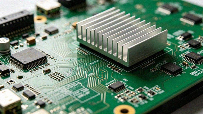
Conducted coupling travels along a conductor, so the answer is filtering and a correct return path. Radiated coupling travels through the air, so the answer is distance, orientation and shielding.
A capacitor at the entry of a supply filters the conducted path, while physical separation and a plane between the aggressor and the victim address the radiated one. The two cases call for different measures, and applying the wrong one wastes the component.
Partitioning the Board
Strong and weak signals should occupy separate regions, and so should digital and analog circuits. The purpose is not to eliminate coupling but to make it predictable enough that the remaining measures can handle it.
The partition should follow the signal flow, and every trace that crosses it should be treated as a deliberate decision. A clock line that wanders from the digital region into the analog region has defeated the partition without anyone noticing.
<img src="https://www.gopcba.com/wp-content/uploads/2025/08/16-1-1.png" alt="Filter and protection components placed at a cable entry on a PCB” />
The Power Supply and the Microcontroller
Most of the immunity of a digital design comes from its supply. Filtering the rail at the point where it enters the board, and decoupling each pin locally, keeps the noise generated by the circuit from reaching the rest of the system and keeps external noise from reaching the device.
A supply monitor is a cheap addition that improves behaviour during a transient, and a device that has a defined reset threshold recovers from a disturbance instead of entering an undefined state.
Clock and Crystal Layout
The clock is both a source and a sensitive node. Its edges are fast, which makes it an efficient radiator, and its input is a high impedance oscillator circuit that will pick up whatever is nearby.
The crystal should be placed as close to the pins as the layout allows, with a ground ring around the circuit and the case bonded to that ground. The clock traces should be short, referenced to a plane and kept away from connectors and from the edge of the board.
Grounding and Return Paths
The digital and analog returns should be separated in the layout and joined at one point, normally at the supply. The purpose is to keep the large digital currents out of the reference that the analog circuit uses.
Within the digital region, the opposite rule applies: the return current should follow its signal, and the reference plane should be continuous. A plane that is broken under a fast trace forces the return current to detour and turns the trace into a better antenna.
Unused Pins and Terminations
An unused input that is left floating is a sensitive node. It should be tied to a defined level through a resistor or configured as a driven output, so that it cannot switch on noise and draw current.
Bus lines that leave the board should be terminated in a way that suits their impedance. A series resistor at the driver is often enough to slow the edge and damp the reflection, and it is far more effective than a capacitor added later.
Filtering and Protection at the Interfaces
Every cable that leaves the product is an antenna. The filter belongs at the point where the cable meets the board, so that the noise does not travel across the board before it is attenuated, and the return of that filter must go to a clean ground.
Protection devices belong in the same place, between the connector and the circuit, so that the energy of a transient is diverted before it reaches the device it would damage. The choice of device and the layout of the path to ground are part of the same decision.
Verification Before the Test House
Pre-compliance measurement in the laboratory is far cheaper than a failed formal test. A near field probe over the board during operation identifies the loudest areas, and a current probe on a cable shows whether the emission is common mode or differential.
The layout should be reviewed against these principles before the board is released, with the same attention given to the EMI suppression measures and to the mixed signal partitioning. Where a switching supply is present, the loop layout described under radiated emission from switching regulators sets the floor for the whole design.
Process Control and Verification
On a design of this kind, interference is the item that decides how the rest of the board is arranged. The measurements that matter are the repeatable ones: conductor width and spacing, annular ring, finished hole size, plating thickness and surface finish are all verifiable on a coupon that travels with the panel. Running a first article through the same checks as the production panel confirms that the two agree, and that comparison is the cheapest form of process control available at prototype stage.
Keeping a sample from the panel turns a dispute into a measurement, because the same coupon can be re-examined by both parties without rebuilding the batch.
Process Control and Verification
On a design of this kind, interference is the item that decides how the rest of the board is arranged. The measurements that matter are the repeatable ones: conductor width and spacing, annular ring, finished hole size, plating thickness and surface finish are all verifiable on a coupon that travels with the panel. Running a first article through the same checks as the production panel confirms that the two agree, and that comparison is the cheapest form of process control available at prototype stage.
FAQ
Which of the three elements should be addressed first? The source, because reducing it helps every path at once. Filtering the victim is effective but has to be repeated for each sensitive net.
Is a ground plane enough? No. A plane gives a continuous return path, but a split, a slot or a connector can still let the return current divert and radiate.
How is a problem found before the formal test? By measuring with a near field probe and a current probe during development, and by reviewing the layout against the coupling path rather than only against the design rules.