High Purity Copper Foil In PCB Fabrication
Copper foil is the layer that becomes every conductor on a board, and its properties are usually taken for granted until a fine line etch or a high frequency measurement exposes them. Two foils of the same nominal thickness can behave differently because of the purity of the copper and the way its grains are arranged, and both are set by the way the foil is made.
This article explains what high purity foil is, how the grain structure develops, and where the difference shows up in practice. The focus is on the situations where the extra cost is justified rather than on a general preference for better material.
What High Purity Foil Is
Electrodeposited foil is produced by plating copper onto a rotating drum from a sulphate bath, then peeling the thin layer off as a continuous sheet. The purity is set by the bath chemistry and by the control of the organic additives that regulate the grain size. Foil described as high purity is typically 99.9 percent copper or better, with trace elements held to levels that do not disturb the conductivity or the etching behaviour.
The purity figure is not the only variable. The same bath can produce a fine grained deposit or a coarse one depending on the additives and the current density, and the two behave differently when they are laminated, drilled and etched. A datasheet that quotes only a thickness and a purity is therefore incomplete for a demanding application.
Thickness is the other variable that is often confused with purity. A foil is specified by its weight per unit area rather than by a measured thickness, and the two are related by the density of copper, so a one ounce foil works out at about thirty five micrometres. The same weight can be produced with different grain structures, which is why two foils of the same grade can behave differently in the press and in the etcher.
The surface treatment also deserves attention when the material is specified. A standard foil carries a treatment on the bond side that provides adhesion to the resin and a treatment on the other side that affects the adhesion of the resist. Both dissolve at rates that differ from the copper beneath, so a heavily treated foil etches differently from a lightly treated one, and the difference appears as a change in the trace profile across the panel.
Why Conductivity Matters At The Trace Level
The resistivity of copper rises as impurities scatter the electrons, and a foil with a lower purity therefore carries slightly more resistance for the same cross section. In a wide power trace the difference is small compared with the design margin, but in a narrow signal trace that runs a long distance the resistance affects the attenuation and the delay.
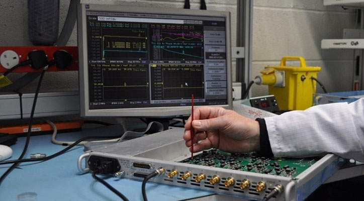
For a high frequency trace the conductor loss is concentrated near the surface, so the roughness of the foil matters as much as its purity. A smoother foil reduces the path length that the current follows and lowers the loss at high frequency. Where a link budget is tight, the combination of purity and low profile is what buys the margin, and the difference can be measured on a test coupon rather than argued from a datasheet.
Etching Fine Features
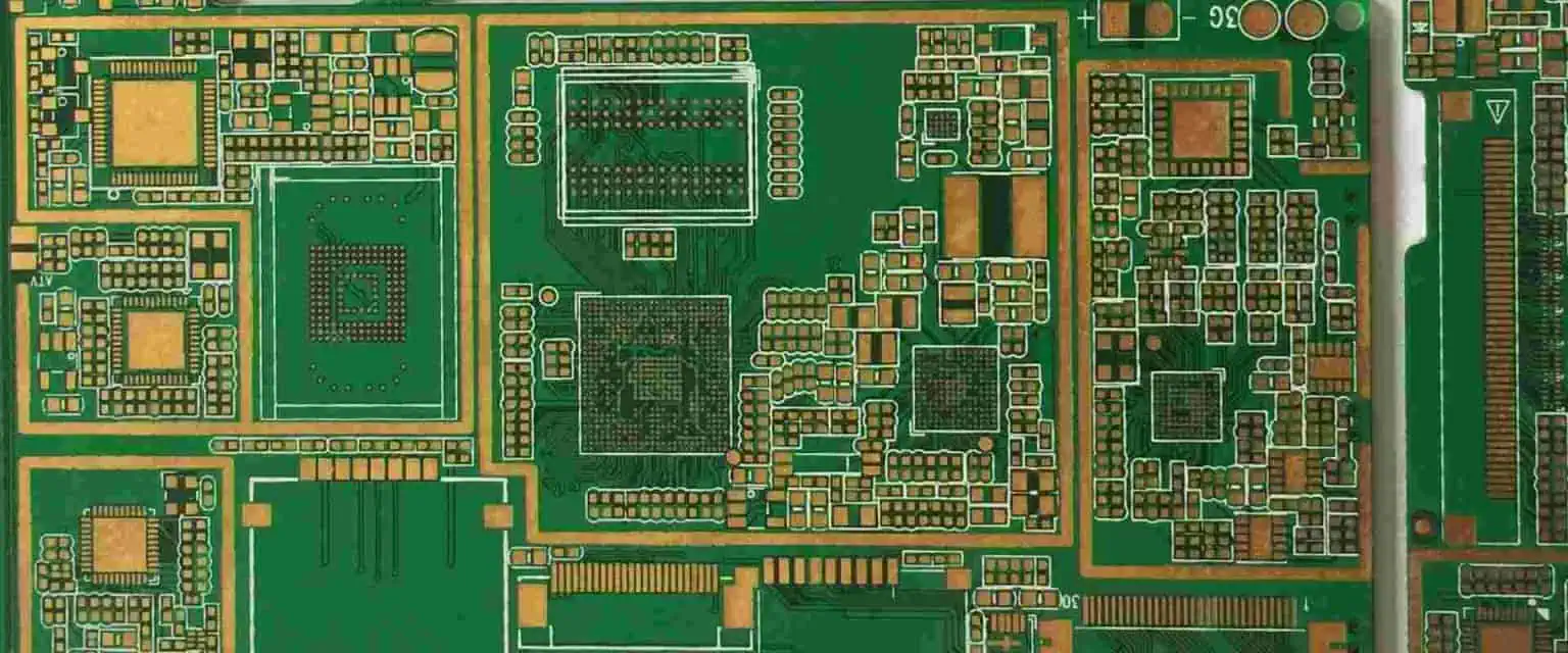
Etching removes the copper that is not protected by the resist, and it works sideways as well as downwards. The ratio between the sideways and the downward removal determines the cross section of the finished trace, and a foil with a fine, uniform grain etches more predictably than a coarse one, where different regions dissolve at different rates.
For fine features the foil thickness sets the limit. A thinner foil leaves less copper to remove, which allows a narrower trace with a straighter sidewall. That is why high density designs specify a thin foil for the fine layers and accept a heavier foil only where the current demands it. The etchant chemistry and the conveyor speed are the process variables, but the foil is what sets the ceiling on the achievable geometry.

Grain Structure And Mechanical Behaviour
The grain structure decides how the foil behaves when it is laminated, drilled and bent. A fine, equiaxed grain distributes strain more evenly, so the foil is less likely to crack at a drilled hole or at a sharp corner. A columnar structure, which grows through the thickness of the foil, can separate along the grain boundary under repeated thermal cycling.
Annealing during lamination changes the structure, since the heat allows the grains to grow. A foil that is specified for a fine grain may coarsen during the press cycle if the temperature is at the high end of the range, which is one reason the same foil can behave differently on two fabricators lines. The interaction between foil, laminate and lamination profile is the reason a change of material is worth a qualification run rather than an assumption. The wider stack up considerations are covered under high speed multilayer design and the fabrication process.
Oxidation And Storage
Copper oxidises in air, and an oxide layer on the foil surface interferes with the adhesion to the laminate and with the plating that follows. Foil is therefore supplied with a treated surface, a thin layer of a metal or an organic that protects the copper and provides a mechanical key for the resin. The treatment also affects the etching, because it dissolves at a different rate from the copper beneath.
Storage conditions matter for the same reason. A roll that has been open in a humid environment will have grown oxide at the edges, and the adhesion in those areas will be worse than in the middle of the roll. Where a board shows poor adhesion in a band rather than across the whole panel, the storage of the foil is one of the first things to check.
Where The Extra Purity Pays Off
The first case is a high frequency link where the conductor loss is a significant fraction of the budget. The second is a fine line design where the trace width is close to the limit of the process, and the etch factor decides whether the impedance is met. The third is a high reliability application where thermal cycling is severe, and the grain structure determines how long a via wall survives.
In a general purpose board with wide traces and moderate frequencies, a standard foil is the economical choice and the difference will not be measurable. The decision should follow the same logic as sizing a trace for current: work out what the design requires, then specify the material that meets it, rather than specifying the best material and hoping the design uses it.
FAQ
Does higher purity always mean lower loss at high frequency? Not on its own. Surface roughness can dominate the conductor loss, so a smooth foil of normal purity may outperform a rough foil of higher purity.
Why does a foil behave differently on two fabrication lines? The lamination profile changes the grain structure of the copper. A higher press temperature coarsens the grains and can alter both the mechanical and the etching behaviour.
Is high purity foil needed for a fine line board? Thickness matters more for the achievable trace width, but a fine and uniform grain structure etches more predictably, which helps hold the impedance across the panel.