High Speed PCB Design: Seven Rules That Pay Off
High speed PCB design is less about a special technique than about a set of habits that reduce the number of times a board has to be redone. The seven rules below are the ones that experienced designers apply on every board, whatever the clock rate.
Know How the Board Will Be Made
The designer should understand the process that turns the files into a board. Without it, the layout is drawn to a precision that the process cannot hold, and the cost rises for a benefit that does not exist.
A simple example is the grid. Placing conductors on a coarse grid and using the fabricator default for the drill and the annular ring produces a board that can be built anywhere. A design that depends on the tightest tolerance the shop can offer is a design that cannot be moved.
Believe the Ratsnest
The ratsnest is the set of straight lines that shows which connections are still missing. It is also a map of how difficult the routing will be, and reading it before the first trace is drawn saves hours later.
A dense crossing pattern in one area is a signal that the placement is wrong there, not that the routing needs to be clever. Moving a component is cheaper than threading a trace through a crowd.

Do Not Skip the Schematic
The schematic is a complete, readable description of the circuit, and it is the reference against which the layout is checked. Working without one removes the ability to verify that every connection was made.
A schematic that is correct but confusing is still a liability, because the person reading it will make an assumption. The document that communicates the circuit is the one that prevents the mistake.
Use the Autorouter Carefully
An autorouter is a tool with parameters, not a solution. It can route a dense board if the constraints are set properly, and it produces unusable results if they are left at the default.
Most experienced designers route the critical nets by hand, lock them, and then use the tool for the remainder. The result is a board where the electrical decisions are made by a person and the routine work is done by the machine.
Spend Time on Placement
Placement is the largest single influence on the routing, and it deserves a corresponding share of the schedule. Getting the components into the right relationship makes the routing straightforward instead of heroic.
The checks are simple: connections should not cross unnecessarily, parts that exchange signals should be close, thermal sources should be separated from sensitive devices, and the connectors should be where the cables arrive.
<img src="https://www.gopcba.com/wp-content/uploads/2026/08/word-image-24809-2.png" alt="Via and fanout detail on a dense high speed board” />
Vias Cost More Than They Look
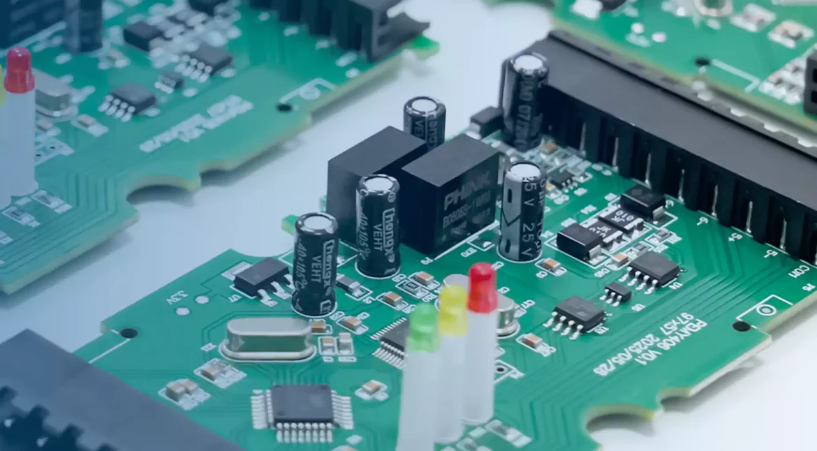
Every via adds inductance, takes routing space on the layers it passes through, and increases the probability of a defect. A design with many vias is a design with many opportunities for a fault.
An aspect ratio of about six to one can be produced almost anywhere. Designing beyond that limits the number of shops that can build the board and increases the price, often for a benefit that a change in placement would have provided anyway.
Take the Design Rule Check Seriously
The check reports what the rules say is wrong, and the rules are set from the capability of the selected fabricator. Every reported error should be either corrected or understood and documented.
A long list of warnings is also information about the layout. If a board generates hundreds of marginal reports, the geometry is probably tighter than it needs to be, and the same result could be achieved with fewer exceptions.
Keep the Stackup Simple
A stackup that is symmetrical, uses standard dielectric thicknesses and keeps the same construction on both sides of the centre is easier to build and behaves more predictably. The gain from a complex stack is smaller than the risk it introduces.
The layer assignment should be planned rather than discovered. Power and ground planes, the layers that carry the fast signals and the layers that carry the slow ones should be decided before the routing begins, using the manufacturability guidance as the constraint.
Length and Delay
Matching the length of two paths is only meaningful if the delay per unit length is the same. A pair that is routed on two different layers can be equal in length and unequal in delay.
Where a match is required, the constraint should be expressed in time rather than in distance. The serpentine that adds the length should be gentle, because a meander that couples to itself changes the impedance it was meant to preserve.
What the Rules Have in Common
Each of the seven rules reduces the number of unknowns. Knowing the process, reading the ratsnest, working from a schematic and checking the result all remove the possibility of a mistake that is only found after the board is built.
The fanout rules and the via rules are the practical form of the same idea for a dense board, and they are worth reading before the placement is fixed rather than after.
Simulation Where It Pays
Simulation is not necessary for every net. It becomes valuable wherever the behaviour is not obvious: a high current path, a controlled impedance route, a connector with a large discontinuity or a thermal problem.
The result should be recorded with the design so that the next revision starts from the same assumptions. A simulation that is not documented is repeated, and the repetition is what makes it feel expensive.
Reviewing Your Own Work
The most effective review is the one done by someone else, but a self review against a checklist catches a surprising amount. Connectivity, silkscreen, mask openings, drill table and the outline are the items that fail most often.
The layout should be examined at the zoom level where a human will see it. A pad that looks correct at full zoom is often found to be touching a neighbour when the view is reduced to the size of the assembled board.
Handover and Output
The output package should leave nothing to be inferred. The files, the drawing, the stackup and the assembly data together describe the board, and a note in an email is not part of the package.
Where a change is made after the release, the revision should be recorded and the affected documents updated. A board built from a mixture of two revisions is the most difficult fault to diagnose, and the only defence is the record.
Reviewing a Dense Board
A dense high speed pcb design is reviewed in slices rather than as a whole. One pass looks at the power, another at the clocks, another at the interfaces and another at the manufacturing data, and each pass has a defined question to answer.
Reviewing everything at once produces a general impression rather than a list of findings. The slice approach is faster, and it produces items that can be closed individually before the board is released.
FAQ
Is an autorouter worth using? Yes, for the non critical part of a dense board, provided the constraints are set properly and the result is reviewed by a person.
Why avoid small vias? Because they limit the number of fabricators that can build the board and increase the defect rate. A larger via is usually available with a small change in placement.
How much of the schedule should placement take? A large fraction on a dense board. Placement decides the routing, and the routing decides whether the electrical rules can be met.