Test Point Design And Coverage For In Circuit Test
A test point is the surface where a spring loaded probe touches the board, and it is the only interface between the product and an in circuit tester. Its size, its spacing, and its position decide whether a fixture can be built at all, how much force that fixture applies to the board, and how much of the circuit can actually be tested. Test points are usually added at the end of the layout, which is exactly when they are most expensive to place well.
This article explains what a bed of nails fixture needs from the layout, how test points are sized and spaced, how coverage is decided, and how the requirements differ for a flying probe.
What A Bed Of Nails Fixture Needs
The fixture holds a probe for every node that will be contacted, and each probe is a spring loaded pin that compresses against the board. A typical probe requires between one hundred and two hundred grammes of force, so a fixture with two thousand probes applies several hundred kilogrammes to the panel, which has to be supported across its whole area by a backing plate and by tooling pins in the rails. The panel therefore contributes mechanically to the test, not only electrically.
On the electrical side the fixture needs a mask free, flat pad for each probe, with a surface that is not covered by coating and not contaminated. The probe also needs room to approach the pad without touching a component, and the fixture needs a grid on which the probes can be placed, because a probe cannot be positioned arbitrarily close to its neighbour. The two common grids are the traditional two and a half millimetre pitch and the finer one and a quarter millimetre pitch used for dense boards.
Sizing And Spacing The Test Points
A test point is normally a rectangular or circular pad of bare copper with no solder mask over it, and its size follows the probe that will use it. A standard probe needs a target of about a millimetre, a fine pitch probe can work down to half of that, and a probe that is asked to contact a pad smaller than its specification will produce intermittent readings that are difficult to diagnose. Copper that is covered by mask is not a test point, because the probe will not penetrate the film reliably and the contact resistance will vary from board to board.
The spacing rules are the other half of the design. Probes must be far enough apart for the fixture to drill the probe holes, which means a test point pitch that follows the grid rather than the layout, and each test point needs a clearance from tall components so that the probe can descend vertically onto the pad. A probe that lands on a via is a common compromise, and it works if the via is not tented and if the fixture can tolerate the small target, but the contact is less reliable than a dedicated pad and the via is also a mechanical feature that can be damaged by the probe.
Deciding What To Test
Coverage is a design decision rather than a tester setting. The nets that justify a test point are the power rails, the ground, the nets that connect to a connector, and the nets that can be shorted by a process fault such as a solder bridge, because those are the failures the tester is best at finding. A net that is buried under a ball grid array, or that is routed between two layers with no access, cannot be probed directly and has to be tested through a boundary scan or a functional test instead.
The number of test points also has an economic limit. Every probe adds cost to the fixture, every additional node adds test time, and a board with several thousand test points may need a fixture that costs more than the product it tests. The usual approach is to allocate test points to the nets with the highest value and to cover the remainder with a combination of optical inspection and functional test. The nodes that are chosen should be listed and given names, because the test engineer will build the program from that list rather than from a picture of the layout.
Layout Rules For Test Points
Test points belong on one side of the board, normally the solder side, because a fixture that probes both sides is much more expensive and much harder to support. They should be placed on the grid, kept clear of tall components by several millimetres, and kept out of the areas where a shield, a connector, a stiffener, or a label will be present. Where a test point is placed near the board edge, the fixture needs the panel rail and the tooling holes to locate it, so the rail design and the test point layout are decided together.
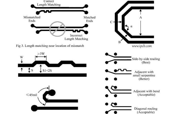
The routing of the test point is worth as much attention as its position. A short stub from a signal trace to a test pad adds capacitance and creates a reflection, which matters on a high speed net, so the stub should be as short as possible or the test point should be placed on a node that already exists. A test point placed directly on a controlled impedance line changes the local geometry, and on a differential pair it can unbalance the two halves. Where the test point is unavoidable on such a net, it is usually placed on a via rather than on a length of trace.
Flying Probe And Its Different Requirements
A flying probe places two or more moving heads on the board instead of a fixed bed of nails, so it needs no fixture and no grid. The pads can be smaller, the pitch can be tighter, and the same program can test a prototype and a production panel without any tooling cost, which makes it the natural choice for low volume work and for first articles. The price is time: each node is visited sequentially by a moving head, so a board with a thousand nets takes far longer than it would on a bed of nails.
The mechanical requirements are different as well. A flying probe needs an accurate fiducial to locate the board, a flat surface to reference, and enough clearance for the heads to reach every pad, which means that a tall component can block a large area. The probe also presses on the pad, so a thin or weakly supported board can flex under the load, and the test points should be positioned where the board is supported. The general design rules that make a board easy to handle are described under layout decisions that affect production.
Documentation And Handover To Test
The test point list is the document that transfers the design intent to the test engineer, and it should carry the net name, the coordinate, the pad size, the side, and any note about the signal that must not be disturbed. The list is generated from the layout rather than written by hand, so that the coordinates match the artwork exactly, and it is checked against the netlist before the fixture is ordered.
The fixture itself is built from that list, and its cost and lead time are a function of the number and the pitch of the probes. A layout that respects the grid, uses a consistent pad size, and keeps the probe areas clear will produce a fixture that is cheaper, faster to build, and more reliable in use. The pad geometry that the test points follow is described under pad design standards, and the panel features that locate the fixture under board outline and mounting design.
FAQ
Can a via be used as a test point? It can, provided it is not tented and the fixture can accept the smaller target. The contact is less consistent than on a dedicated pad, and the probe can damage a small via, so a dedicated pad is preferred where space allows.
Should test points be placed on both sides of the board? Only when there is no alternative. Probing both sides doubles the fixture complexity and makes it harder to support the board against the probe force.
How many test points does a board need? Enough to cover the nets whose failure the tester can detect, which usually means power, ground, connector nets, and nets that are prone to bridging. The rest are covered by inspection and functional test.