LED Assembly Thermal Design and Reflow
An LED assembly is a thermal design with a light attached. The junction temperature sets the light output, the colour and the life, and the board is the path that removes the heat.
Why the Junction Temperature Matters
The light output falls as the junction temperature rises, and the colour shifts with it. The life falls steeply, so a design that runs ten degrees cooler can last noticeably longer.
The junction temperature is not measurable directly, so it is calculated from a thermal resistance and a measured board or case temperature. Our thermal measurement notes describe how the measurement is taken.
The Path Through the Board
The heat leaves the package through a thermal pad on the underside and enters the board. From there it spreads laterally and leaves through the board surface, the housing or a heatsink.
The dielectric between the pad and the inner layers is the bottleneck, so the design uses thermal vias under the pad and a copper area around them. Our thermal via notes describe the arrangement.
Metal Core and Ceramic Boards
Where the heat is high, an aluminium or a copper core board removes the dielectric from the path and spreads the heat over the whole panel. The dielectric is a thin insulating layer instead of the laminate.
A ceramic substrate performs better still and it costs more and it is more brittle. The choice follows the power density rather than the cost per board alone. Our metal core notes describe the comparison.
Reflow of LED Assemblies
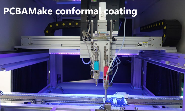
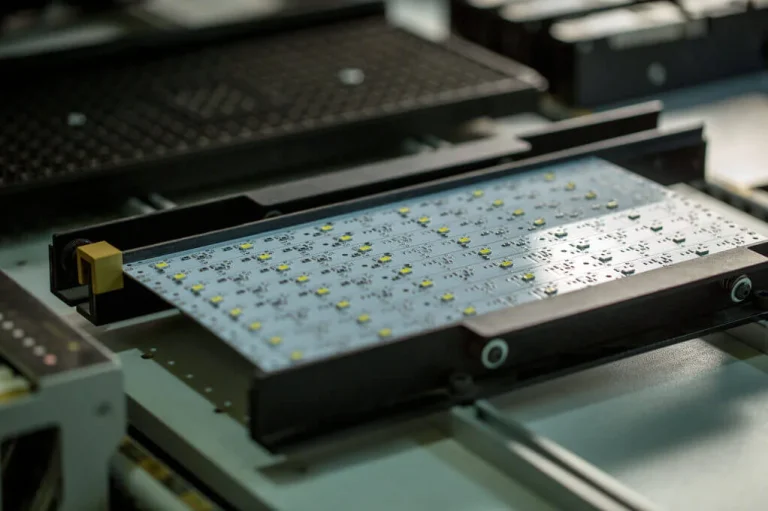
The package is sensitive to moisture and to thermal exposure, and the profile must stay inside the limits the supplier specifies rather than inside a general lead free window.
The board’s thermal mass delay also means the pad under the LED reaches the peak later than the rest of the board, so the measurement should be taken there. Our thermal mass notes describe the measurement.
Optical Considerations
The solder mask colour around an LED affects the light that is reflected back, and a white mask is used where the reflection matters. The finish and the mask both change the colour of the light that leaves the assembly.
Those are design decisions rather than process decisions, and they should be stated with the assembly rather than left to the fabricator.
Layout for Heat Spreading
The copper around the LED spreads the heat before it leaves the board, so the area matters as much as the via count. A large copper area at the same voltage potential is the usual arrangement.
Where the copper is split by the routing, the spreading is interrupted and the temperature rises locally. Our copper balance notes describe the patterns that spread heat without unbalancing the board.
Verification
The verification is the board temperature measured at the worst case drive current and ambient, converted to a junction temperature with the supplier’s thermal resistance.
The measurement should be taken in the finished housing, because the housing is usually part of the thermal path. Our heatsink notes describe the interface that connects them.
Process Control and Verification
On a design of this kind, thermal via is the item that decides how the rest of the board is arranged. Documenting the assumption is part of the design work, and a short note on the drawing prevents a question that would otherwise arrive a day later and cost a day of schedule. The process window is set by the narrowest step in the flow, so an improvement anywhere else shows up as margin rather than as yield until that step is addressed.
A short note on the drawing about handling, storage or packaging is often worth more than an extra decimal place on a tolerance. Where a value sits close to a process limit, the drawing should say so, since the shop can then open the process window rather than working to a nominal figure that carries no tolerance.
A stack-up that is drawn rather than described removes most of the ambiguity from a quotation, and it lets the fabricator price the board against the dielectric and copper weights that will actually be used. Where the requirement is not written down, the shop supplies its own default, and the default is chosen for the process rather than for the design.
The measurements that matter are the repeatable ones: conductor width and spacing, annular ring, finished hole size, plating thickness and surface finish are all verifiable on a coupon that travels with the panel. Running a first article through the same checks as the production panel confirms that the two agree, and that comparison is the cheapest form of process control available at prototype stage.
Process Control and Verification
On a design of this kind, thermal via is the item that decides how the rest of the board is arranged. Documenting the assumption is part of the design work, and a short note on the drawing prevents a question that would otherwise arrive a day later and cost a day of schedule. The process window is set by the narrowest step in the flow, so an improvement anywhere else shows up as margin rather than as yield until that step is addressed.
A short note on the drawing about handling, storage or packaging is often worth more than an extra decimal place on a tolerance. Where a value sits close to a process limit, the drawing should say so, since the shop can then open the process window rather than working to a nominal figure that carries no tolerance.
A stack-up that is drawn rather than described removes most of the ambiguity from a quotation, and it lets the fabricator price the board against the dielectric and copper weights that will actually be used.
Process Control and Verification
On a design of this kind, thermal via is the item that decides how the rest of the board is arranged. Documenting the assumption is part of the design work, and a short note on the drawing prevents a question that would otherwise arrive a day later and cost a day of schedule. The process window is set by the narrowest step in the flow, so an improvement anywhere else shows up as margin rather than as yield until that step is addressed.
A short note on the drawing about handling, storage or packaging is often worth more than an extra decimal place on a tolerance.
Process Control and Verification
On a design of this kind, thermal via is the item that decides how the rest of the board is arranged. Documenting the assumption is part of the design work, and a short note on the drawing prevents a question that would otherwise arrive a day later and cost a day of schedule. The process window is set by the narrowest step in the flow, so an improvement anywhere else shows up as margin rather than as yield until that step is addressed.
A first article check confirms that the process and the drawing agree on the points listed above, and that the coupon data supports the values used in the design.
Where a measurement falls outside the expected window, the sample is retained so that the cause can be established before the balance of the batch is released.
FAQ
Is a metal core board always better for LEDs? It is better where the power density is high and the board is a single layer. It is not suited to a dense control circuit on the same board.
Can the light output be used to estimate the junction temperature? It changes with the temperature and it also changes with the drive current and the age, so the thermal measurement is the more reliable route.
What does gopcb provide for LED assemblies? We provide thermal path design with vias and spreading copper, material selection between laminate, metal core and ceramic, profiles developed to the package limits, measurements taken at the package pad and in the housing, and layout that spreads heat without unbalancing the board.