EMC Shields, Gaskets and Frame Grounding
Where a board has to be shielded, the enclosure, the frame and the gasket form the shield. A gap in the path is the difference between an attenuation figure and a product that fails the radiated emission test.
What the Shield Has to Do
The shield reflects and absorbs the field, and the current induced in it has to return to its source through a continuous path. The path is the shield itself and the connections to the ground.
At high frequency the current does not take the shortest route; it follows the path of least impedance, which hugs the seam. That is why the seam matters more than the sheet. Our EMI notes describe the layout measures that support it.
Gaskets
A conductive gasket fills the gap between the shield and the ground surface and it makes the connection continuous. Its properties are the impedance and the compression it needs.
A gasket that is compressed beyond its range loses its elasticity and a gasket that is not compressed enough has a high impedance. The compression should be defined and the housing should produce it. Our coating notes describe a surface treatment that would interfere with the contact.
Frames and Clips
A board level shield is often a stamped frame soldered to the board with a lid clipped to it. The frame is the reliable part of the connection; the clip is the part that varies.
The clip must touch at intervals that are a fraction of a wavelength at the highest frequency of concern. A clip with widely spaced fingers behaves as a slot antenna above a certain frequency. Our high speed notes describe the frequency range.

Grounding to the Board
The frame is soldered to a ground area with vias close to the connection, so that the current leaving the frame enters the ground plane without a long path.
A frame soldered to a pad without vias nearby forces the current to travel along the surface. The vias should be placed at the frame footprint rather than distributed elsewhere. Our placement notes describe a related return path question.
Apertures and Cables
Every opening in the shield radiates, so the size of the opening sets the frequency above which the shield is ineffective. Ventilation holes and connector cut-outs are the usual offenders.
A cable leaving the shield carries the current out and it becomes part of the antenna unless it is filtered or grounded at the boundary. Our ferrite notes describe one of the measures.
Assembly Considerations
The shield must be placed by the machine and it must survive the reflow. A frame that is warped or a lid that is fitted by hand introduces a variable that the design cannot control.
The compression of the gasket has to be produced by the assembly, which means the stack and the tolerances have to be calculated. Our mounting notes describe the same stack analysis.
Verification
The verification is a near field scan of the board with the shield fitted, and a radiation measurement on the complete product.
Where the board passes and the product fails, the shield and the enclosure together are the cause rather than either alone. Our quality notes describe how the result is recorded.
Additional Considerations for This Build
Practical attention to grounding via pays for itself here, because it decides whether the finished board behaves as the drawing intended. Where the requirement is not stated on the fabrication drawing or in the assembly notes, the shop has to assume a default, and that default is rarely the value the design was simulated with. Stating grounding via explicitly, together with the tolerance that applies, removes the assumption and keeps the result predictable from batch to batch.
Process Control and Verification
On a design of this kind, shield is the item that decides how the rest of the board is arranged. A stack-up that is drawn rather than described removes most of the ambiguity from a quotation, and it lets the fabricator price the board against the dielectric and copper weights that will actually be used. Where the requirement is not written down, the shop supplies its own default, and the default is chosen for the process rather than for the design.
The measurements that matter are the repeatable ones: conductor width and spacing, annular ring, finished hole size, plating thickness and surface finish are all verifiable on a coupon that travels with the panel. Running a first article through the same checks as the production panel confirms that the two agree, and that comparison is the cheapest form of process control available at prototype stage.
Keeping a sample from the panel turns a dispute into a measurement, because the same coupon can be re-examined by both parties without rebuilding the batch. Reviewing the design before the data is released is cheaper than correcting it after the panel is in the tank, because every step downstream inherits the decision made at the front end.
Documenting the assumption is part of the design work, and a short note on the drawing prevents a question that would otherwise arrive a day later and cost a day of schedule. The process window is set by the narrowest step in the flow, so an improvement anywhere else shows up as margin rather than as yield until that step is addressed.
Process Control and Verification
On a design of this kind, shield is the item that decides how the rest of the board is arranged. A stack-up that is drawn rather than described removes most of the ambiguity from a quotation, and it lets the fabricator price the board against the dielectric and copper weights that will actually be used. Where the requirement is not written down, the shop supplies its own default, and the default is chosen for the process rather than for the design.
The measurements that matter are the repeatable ones: conductor width and spacing, annular ring, finished hole size, plating thickness and surface finish are all verifiable on a coupon that travels with the panel. Running a first article through the same checks as the production panel confirms that the two agree, and that comparison is the cheapest form of process control available at prototype stage.
Process Control and Verification
On a design of this kind, shield is the item that decides how the rest of the board is arranged. A stack-up that is drawn rather than described removes most of the ambiguity from a quotation, and it lets the fabricator price the board against the dielectric and copper weights that will actually be used. Where the requirement is not written down, the shop supplies its own default, and the default is chosen for the process rather than for the design.
A first article check confirms that the process and the drawing agree on the points listed above, and that the coupon data supports the values used in the design.
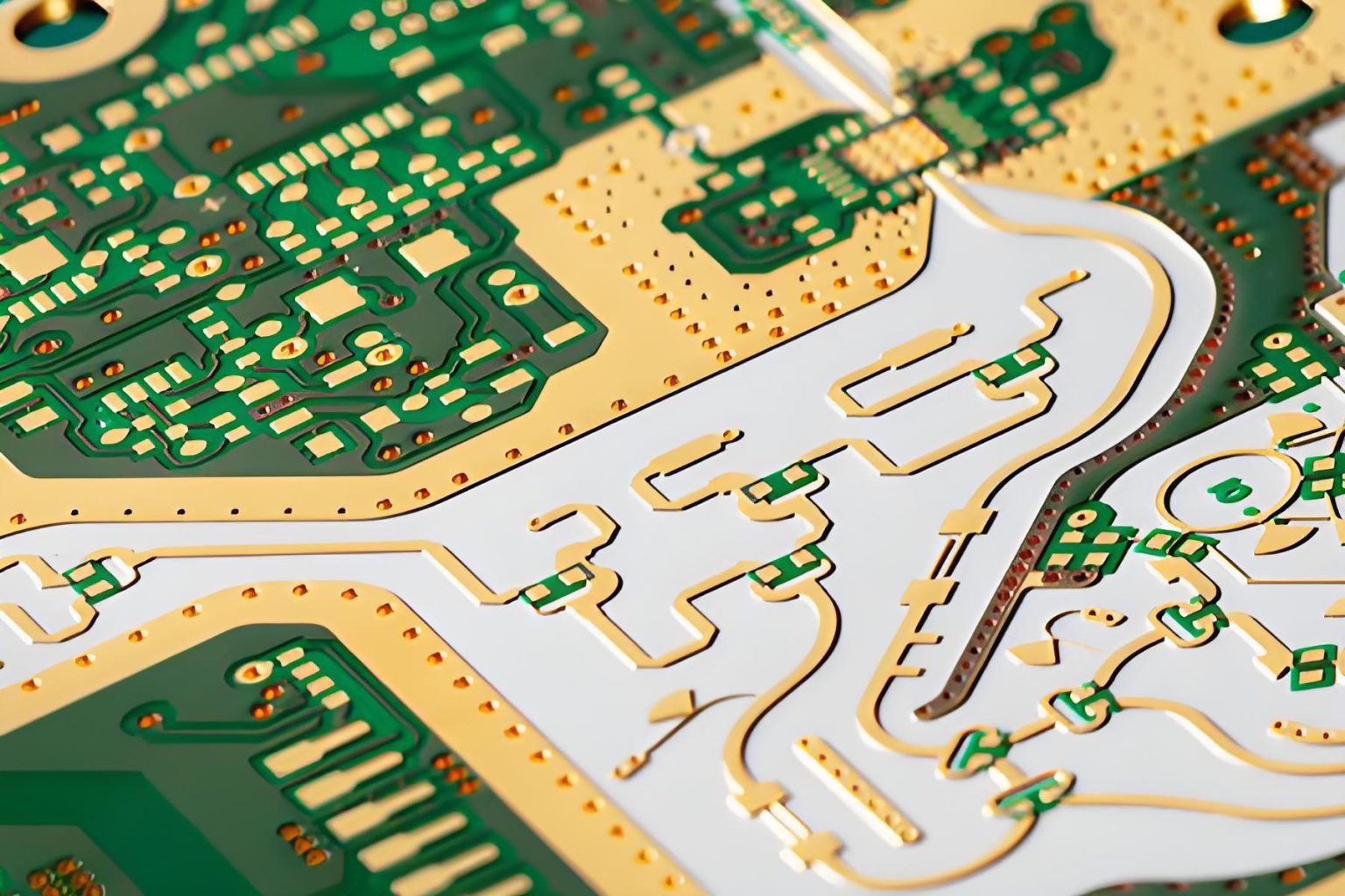
Where a measurement falls outside the expected window, the sample is retained so that the cause can be established before the balance of the batch is released.
FAQ
Does a shield need to be connected on all sides? The connection must be continuous at the frequencies involved. A clip on two sides with a wide gap behaves as a slot at high frequency.
Can a coating be applied under the frame? It can, and it adds an insulating layer where the connection is needed. The contact area should be kept clear.
What does gopcb provide for EMC shielding? We provide shield and gasket selection with a defined compression, frame and clip design with finger spacing set by frequency, ground vias at the frame footprint, aperture and cable boundary review, placement and stack analysis, and near field and radiated verification.