Embedded Processor Board Design for Peripheral Rich Products
Once a processor has been selected, the board around it becomes the real engineering problem. A peripheral rich device presents dozens of interfaces, several supply rails, a memory bus and an escape pattern that dictates the stackup. Embedded processor board design for these products is a study in planning: almost every difficulty can be avoided by deciding the interface map and the layer stack before routing begins.
Interface Planning Before Layout
Build a complete interface map first: every controller, its target pins, its data rate, its power domain and its reference clock. Assign pin groups to physical board regions so that interfaces that share a clock domain stay close together and interfaces that must be isolated are physically separated. This map becomes the placement plan and the basis for the stackup decision.
Include the pins that seem unimportant. Boot configuration straps, mode selects and reset sources are often forgotten until bring-up, at which point they need to be accessible. Reserve header pins or test pads for them during planning, when there is still space, rather than after the board area is committed to connectors and regulators. Reviewing the pin map with escape routing and fanout constraints in mind keeps the plan realistic.
DDR Memory Routing Fundamentals
Memory is usually the most demanding interface on the board. The data group must be length matched within a tight tolerance, the address and command group must match within a looser one, and the differential clock must be routed as a pair with controlled impedance. All of it needs a continuous reference plane, which means no plane splits beneath the bus.
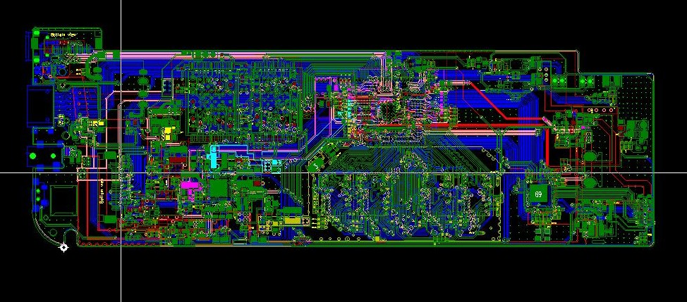
Route the bus on a single layer where possible and keep the via count low and consistent. Vias add inductance and stub effects, and an uneven via pattern produces skew that no length matching can compensate for. Where the bus must change layers, change all signals in the group in the same place so that the discontinuity is shared rather than random. The techniques are the same ones described for serpentine routing and length matching on other high speed interfaces.
High Speed Serial Links
Serial links such as PCI Express and SATA bring their own requirements: strict differential impedance, a defined loss budget, and an alternating current coupling capacitor placed close to the transmitter. Route them on the layer adjacent to a solid ground plane, keep them away from switching regulators, and avoid layer changes unless the stackup supports a well matched transition.
Reference clock quality determines whether the link trains at the expected speed. Place the reference source close to the processor, filter its supply, and keep the differential clock pair short and symmetrical. On boards with several serial links, verify that the reference clocks do not share a noisy supply with the memory or the switching converters.
USB, Ethernet and Storage Interfaces
Consumer interfaces are more forgiving than memory, but they are not free. USB 2.0 needs a matched pair with a defined impedance, Ethernet needs matched pairs plus attention to the magnetics and the chassis ground connection, and storage interfaces need short, well referenced traces with adequate decoupling at the connector. Each of these can be routed on a two layer board when the geometry allows, provided the return path is continuous.
Protection components belong at the connector, not at the processor. Electrostatic discharge events enter through the connector pins, so the clamp must be the first thing the transient meets. Place the device within a few millimeters of the connector, keep its ground connection short, and avoid routing the protected signal past unprotected circuitry. Filter components should sit between the clamp and the processor.
Power Delivery for a Multi Rail Processor
A peripheral rich processor typically needs a core rail, a memory rail, one or more input and output rails and separate analog supplies. Plan the power tree as a system: which converter feeds which rail, what the sequencing order is, and how the current returns to the source. Keep each switching converter compact, place its inductor away from sensitive interfaces, and give every rail a defined decoupling strategy.
Sequence the rails according to the datasheet and verify the order with a scope rather than by inspection. Where rails share a copper pour, keep them separated so that the return currents of a high current rail do not flow beneath a sensitive one, following power plane splitting rules. Provide a way to measure each rail at the pin, because a rail that looks correct at the regulator may be out of tolerance at the load.
Clocking and Reset Architecture
Clock architecture is easy to under-plan on a board with many interfaces. Identify every device that needs a reference, decide whether it is fed from the processor, from a dedicated oscillator or from a clock generator, and confirm that the jitter requirement of each interface is met by the chosen source. Sharing one oscillator across several devices is efficient but can spread noise between them.
Reset architecture deserves a separate plan as well. Define what resets the processor, what the processor resets, and in what order. A supervisor that holds the processor in reset until every rail is valid prevents the most common class of intermittent boot failure, and a clearly documented reset tree prevents a peripheral from starting before the processor can configure it.
Bring-Up Strategy for Complex Boards
Bring-up should be staged: verify the rails and the sequencing, confirm the reference clocks, establish a debug interface, then test each peripheral individually before running the full application. Boards with many interfaces fail in ways that are difficult to isolate when everything is enabled at once, and a staged approach reduces the search space to one subsystem at a time.
Provide the debug access that the staging requires. A serial console, a JTAG or SWD header and a way to force the boot mode are the minimum. Keep these connections on the schematic even when they will not be populated in production, so that a field return can be investigated with the same tools used in the laboratory.
Cost Control and Layer Planning
Layer count is the largest single cost lever on a processor board. Plan the stackup around the escape pattern and the critical interfaces, then route the remaining signals on the layers that are left. Adding a pair of layers to accommodate a few hundred general purpose connections is usually cheaper than adding assembly steps or accepting a lower yield.
gopcb builds processor boards with high speed interfaces and can review the stackup, the power tree and the memory routing before the design is released, since those decisions are interconnected and expensive to change later. A review at that point typically shortens the first prototype cycle more than any subsequent optimization.
FAQ
How many layers does a processor board with DDR memory need? Four layers is the practical minimum when the memory bus can be referenced to a solid plane, and six layers is common when the bus is wide or when several serial links share the same area. The escape pattern of the processor usually decides the answer.
Can the memory bus be routed on the same layer as the serial links? It can, but the two should not run parallel over a long distance on adjacent layers without a ground plane between them. Crosstalk between a wide parallel bus and a serial link is easy to create and difficult to diagnose.
What is the most common bring-up failure? Missing or incorrect power sequencing, followed by a clock that does not start because of a wrong load capacitor value. Both are avoided by verifying the rails and the reference frequency before powering the processor for the first time.