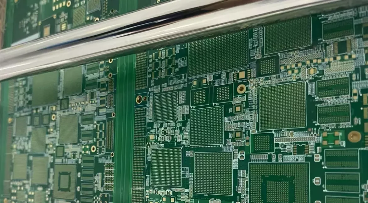
Thermal Via Placement for Heat Paths in a PCB
A thermal via is a hole in the board that was put there to move heat rather than to connect a net. The idea is simple, and the design decisions around it are not, because a via array changes the electrical plane, the solder joint above it and the mechanical stiffness of the laminate at the same time.
Most thermal problems on a board are resolved by spreading heat sideways and then passing it to the other side, and the via array is the passage between the two. Getting the array right is often the difference between a component that runs cool and one that derates itself within minutes.
How Heat Leaves a Package
Heat leaves a component by three routes at once: through the leads, through the body into the air, and through the thermal pad into the board. The third route is usually the dominant one for a modern package with a exposed pad, and it depends entirely on what the board does with the heat once it arrives.
A pad that sits on a small area of copper, on an outer layer only, has nowhere to send the energy. The same pad connected to an array of vias that opens into an internal plane behaves as if it were attached to a large heat sink, because the plane is the heat sink.
Vias as a Heat Path
Each via is a cylinder of copper with a thin wall, and its thermal resistance falls as the wall gets thicker and the barrel gets shorter. Plating thickness matters more than most designers expect, because a barrel that is plated to 20 micrometres carries far less heat than one plated to 35 micrometres.
The barrel is also in series with the pad on the top and the copper on the bottom, so the interface between them is part of the path. That is why an unfilled via under a thermal pad loses much of its value: the void in the middle of the joint and the air in the barrel both interrupt the path that was designed.
Diameter, Pitch and Count
Many small vias generally outperform a few large ones for the same copper cross section, because the surface area available for heat transfer into the surrounding copper is larger. A typical array uses vias between 0.2 and 0.3 millimetres in finished diameter on a pitch of about one millimetre.
The pitch is set by the requirement that paste must not wick into the holes on the top side and that the copper between the vias must remain continuous. Bringing the vias closer than half a millimetre risks a paste drain during reflow, which is the same mechanism that governs any open aperture inside a pad.
Copper Area Around the Array
The vias are only the beginning of the path, and the copper they land on decides how much heat can be moved away. A wide plane on the opposite side, or a heavy copper area on an inner layer, gives the energy somewhere to spread, while a narrow trace from the last via limits the whole arrangement.
Where the plane is on an inner layer, the connection between the via and the plane should be solid rather than relieved. Thermal reliefs exist to make soldering easier on through hole pads, and they are counterproductive on a via whose purpose is conduction, so the array should be excluded from relief rules.
Voiding Under the Pad
An unfilled via opens a path for gas from the barrel into the molten joint, and the result is solder voiding that reduces the contact area between the pad and the component. Voiding under a thermal pad is worse than in a signal joint, because the joint itself is the heat path.
The usual remedy is to fill and cap the array so that the top surface is solid copper, which allows the paste to form a full contact area and removes the gas source. Where filling is not used, the void percentage should be measured on a sample and the thermal performance assessed against the measured figure rather than the ideal one.
Via in Pad and the Stencil
When the vias are capped, the pad becomes a normal surface and the stencil aperture can be calculated from the paste volume the joint requires. When they are not capped, the aperture should be divided into smaller openings that avoid the holes, which reduces the total volume but prevents the paste from draining.
The two approaches produce different joints and different thermal resistance, so the choice belongs in the design review rather than in the fabrication notes. This is one of the points where the fabrication decision described in copper plating and via filling directly determines whether the thermal design works.
Interaction With Plane Layers
An array of vias passing through a plane has to be handled in the plane data, because each hole removes copper from the layer that is supposed to spread the heat. Clustering the vias in a tight grid keeps the removed area small, while scattering them across the plane interrupts the current paths of the net the plane carries.
Where the plane carries a high current, the array should be placed so that the current path is not narrowed below the design value. The thermal and electrical functions of the same copper have to be checked together, which is the same coordination required for thermal management design in general.
Electrical Trade-offs
A thermal via array connected to a ground plane also creates a path for noise and for stray capacitance to that plane. On a high speed signal the same structure would be a controlled impedance feature, so a thermal array should never be placed under a signal pad without checking the effect.
Where the array is connected to a plane that is not the ground of the component, the resulting loop can couple switching noise into the plane. The usual solution is to tie the array to the ground plane of the device that generates the heat, keeping the return path local and short.
Assembly Considerations
The array affects the way the board heats during reflow, because copper conducts heat away from the joint that is trying to form. A thermal pad on a large plane needs a longer soak or a higher local temperature than a signal pad, and that difference is one reason a profile taken on a small coupon does not describe the real assembly.
Solder volume also has to be increased to fill the gap created by the pad and the component, and the aperture is calculated for the volume rather than copied from a similar part. Joints that look acceptable but contain a large void are a common finding under thermal pads, and they are invisible from the outside.
Verification
Thermal performance is verified with a measurement rather than with a calculation, and the measurement is usually the case temperature of the component under load. Comparing that figure with the same measurement on a board without the array is what proves the array is doing the work.
Where a thermal camera is used, the image should be taken after the board has reached steady state, since a board that is still warming produces a flattering pattern. The result belongs in the design record together with the stack up and the copper weights, in the same way that the checks in judging board quality are recorded for a build.
Additional Considerations for This Build
Practical attention to heat spreading pays for itself here, because it decides whether the finished board behaves as the drawing intended. Where the requirement is not stated on the fabrication drawing or in the assembly notes, the shop has to assume a default, and that default is rarely the value the design was simulated with. Stating heat spreading explicitly, together with the tolerance that applies, removes the assumption and keeps the result predictable from batch to batch.
A first article check confirms that the process and the drawing agree on the points listed above, and that the coupon data supports the values used in the design.
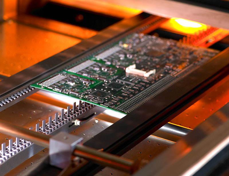
Where a measurement falls outside the expected window, the sample is retained so that the cause can be established before the balance of the batch is released.
A first article check confirms that the process and the drawing agree on the points listed above, and that the coupon data supports the values used in the design.

Where a measurement falls outside the expected window, the sample is retained so that the cause can be established before the balance of the batch is released.
FAQ
How many vias does a thermal pad need? As many as will fit on the specified pitch without compromising paste release, and the count is a starting point that a measurement then confirms.
Should the vias be filled? Under a pad that must be soldered they should be filled and capped, because the alternative leaves a gas path into the joint and a measurable loss of contact area.
Do thermal vias need to be tented on the underside? They should be left open on the side that connects to the plane, so the barrel makes contact with the copper rather than being covered by mask.
Can the array be placed after the design is fixed? Moving an array changes the plane data and the stencil, so it is much cheaper to place it while the layout is still being edited.