Thermal Management in PCB Design: Keeping Parts Cool
Every watt dissipated on a board has to leave it, and the path it takes is decided by the layout rather than by the schematic. A regulator that runs cool in free air can exceed its limit inside a sealed enclosure simply because the copper around it was sized for current rather than for heat. Thermal management is therefore a layout discipline: it is about giving the heat a low resistance route from the junction to the ambient, and about verifying that the route works under the conditions the product will actually see.
Where the Heat Goes
Heat leaves a component by three routes in parallel: conduction through the leads and the thermal pad into the board, convection from the package surface into the air, and radiation from any exposed surface. In most electronic products conduction through the board dominates, because the package is small, the airflow is limited and the board presents a large area to the enclosure.
That is why board design has so much influence. Once the heat is in the copper it spreads laterally and is transferred to the air from a much larger surface, or conducted into a chassis through the mounting hardware. A design that provides a broad copper path and a good connection to the mechanical structure can run a device at a fraction of the temperature rise of a design that leaves it isolated.

Thermal Resistance as a Chain
The path from junction to ambient is a series of thermal resistances: junction to case, case to board, board to ambient, and any interface in between. Adding them gives the total, and multiplying by the dissipated power gives the temperature rise. The exercise is valuable because it shows where the bottleneck lies; improving a link that is already small changes nothing.
In practice the board to ambient term is usually the largest, and it is also the one the layout controls most directly. Interface materials, thermal pads and mounting pressure set the case to board resistance, which is why the mechanical assembly drawing matters as much as the copper geometry. Our notes on PCB thermal design rules work through the chain in more detail.
Copper Area and Heat Spreading
Copper is the heat spreader on most boards, and its performance depends on area and thickness rather than on shape. A large polygon connected to the thermal pad lowers the local temperature by spreading the heat into a bigger region, and the benefit continues to grow until the copper is large enough that the thermal resistance to air becomes the limit.
Thicker copper spreads heat further before the local temperature rises, which is why heavy copper and metal backed substrates are used for high dissipation parts. On an ordinary multilayer board the inner planes do the same job, so a thermal pad connected by a via array into a solid internal plane is often more effective than enlarging a surface polygon. Our notes on embedded copper coin and thermal substrate comparison cover the heavier options.
<img src="https://www.gopcba.com/wp-content/uploads/2026/09/266-2.jpg" alt="Thermal via array beneath a power device pad” />
Thermal Vias and Pads
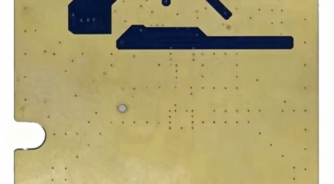
A thermal via is a plated hole used to move heat between layers rather than to carry a signal. Its thermal resistance falls with the plated cross section and rises with length, so a short wide via in a thin board performs far better than a long narrow one. Because a single via has limited cross section, arrays are used, and the array is most effective when it sits directly beneath the thermal pad with the vias on a regular pitch.
Filling and capping the vias matters for the assembly as well as for the thermal path. An open via inside a soldered pad wicks solder away from the joint, leaving voids and reducing the contact area that carries heat. A filled and capped via keeps the pad flat, so the joint forms properly and the thermal path through the solder is continuous.
Junction Temperature Targets
The junction temperature limit in a datasheet is a maximum, not a target. Designing to the maximum leaves no margin for a hot day, a blocked vent or a component tolerance, and it shortens the life of the part even when it does not fail immediately. A working limit well below the absolute maximum, often twenty to forty degrees of margin, is a more realistic design goal.
That margin has to be established at the worst case ambient rather than at room temperature. The enclosure, the position of the board inside it, the neighbouring boards and the airflow all affect the local ambient, and a design verified on an open bench may be quite different once it is installed. Our notes on high temperature PCB materials cover what the laminate itself can take.
Airflow, Enclosure and Derating
Airflow changes the board to ambient resistance dramatically. A surface exposed to moving air transfers heat far more effectively than one in still air inside a closed box, and a design that relies on convection through a vent needs the vent to remain clear in service. Where no airflow is available, the heat has to leave by conduction into the chassis, and the mechanical design becomes part of the thermal solution.
Derating follows from the same reasoning. Reducing the power dissipated is often cheaper than improving the thermal path: lowering a switching frequency, adding a series element to share the load between two devices, or choosing a part with a lower on resistance in the first place. Thermal design and circuit design are not separate activities, and the cheapest watt is the one that is never dissipated.
Verifying the Design
Measurement settles the question. A thermocouple on the device case, or a thermal image of the board under full load, shows the actual temperature rise and where it concentrates, and comparing that result with the calculation identifies which thermal resistance was underestimated. The measurement should be taken at the worst case ambient and at the worst case load, in the enclosure if one exists.
Where a design is marginal, the improvement usually comes from geometry: more copper, a shorter thermal path, a better interface to the chassis or a repositioned device. Component level changes such as a larger package or a lower loss device are also effective, but they are more expensive than rearranging copper that is already there, so the layout options should be exhausted first.
FAQ
How much copper area does a thermal pad need? There is no fixed figure. The required area falls out of the thermal resistance chain, the dissipated power and the acceptable temperature rise, and it grows until the transfer to air becomes the limiting term.
Do thermal vias really help? Yes, when they connect a hot pad to internal planes or to the opposite side of the board. Their benefit depends on the plated cross section, the via length and the number used, and they must be filled and capped if they sit inside a soldered pad.
Is a metal core board necessary for high power? Not always. A well designed multilayer board with heavy copper and a good path into the chassis handles many applications. Metal core and ceramic substrates are chosen when the dissipation or the isolation requirement exceeds what a laminate can carry.