Thermal Via Design Guide
A thermal via is a hole that moves heat rather than a signal. It is placed under a power device, in a ground pad or beneath a component that has to be cooled, and it carries heat from the top surface into the copper planes below. The vias are small, they are usually invisible in the assembled product, and the difference between a good array and a poor one is often the difference between a component that runs at eighty degrees and one that runs at a hundred and twenty.
What a Thermal Via Does
A thermal via is a plated hole that connects a hot pad on the surface to a copper area inside or on the far side of the board. The copper barrel is a path of low thermal resistance compared with the laminate, and the plane it connects to spreads the heat sideways.
The laminate itself is a poor conductor, with a thermal conductivity around a third of a watt per metre kelvin, while copper is near four hundred. A single via of small diameter therefore carries more heat than a large area of laminate under the same temperature difference.
The via does not cool the component, it moves the heat to a place where it can be spread and then removed by convection or by conduction into a housing. The whole path has to be considered, and the weakest link in it sets the junction temperature.
The same structure often serves as the electrical ground connection, which is convenient and also means the thermal design cannot be changed without considering the electrical one.
Thermal Resistance and the Path
Each element of the path has a thermal resistance, and they add in series like electrical resistances. The path runs from the junction to the case, from the case to the solder, from the solder into the pad, through the vias, into the plane and out to the ambient.
The via contribution is only one term, and it is often not the largest. A component with a poor case to solder interface will not be saved by doubling the via count, and a board in still air will not be saved by a plane that has nowhere to dissipate to.
A useful exercise is to estimate each term before the layout is fixed, using the vendor thermal data and a first order calculation for the vias. The estimate identifies the dominant term, and that is where the design effort belongs.
The junction temperature is the case temperature plus the product of the power and the resistance, so a design that runs close to the limit has to include a margin for the ambient and for the age of the product.
Array Geometry and Spacing
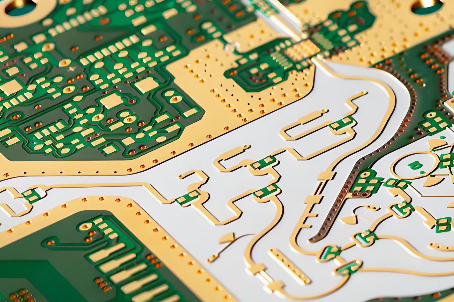
The via array is arranged under the pad, and its geometry is a compromise between the thermal benefit and the soldering risk. More vias lower the thermal resistance, up to the point where the pad becomes a mesh that cannot be soldered reliably.
A common arrangement is a grid with a pitch of about one millimetre and a via diameter of about 0.3 mm, which leaves enough copper between the holes for a good solder joint. The array should cover the area of the pad that is under the component.
The vias should be placed where the heat is generated, which is not always the centre of the package. A device with the heat concentrated in one corner benefits from an array that is shifted toward that corner.
Vias that are also used as signal connections should be excluded from the thermal array, because a signal via in a power pad couples noise and complicates the routing. The power integrity work should reserve the array for the thermal and ground function.
Copper Thickness and Plating
The barrel of the via is a plated copper tube, and its thermal resistance depends on the cross sectional area of the copper rather than on the hole diameter. A thick plating in a small hole can beat a thin plating in a large one.
A plating of twenty five microns in a 0.3 mm hole gives a barrel area that is easy to calculate and that behaves predictably. A very thin plating of a few microns, which is acceptable for a signal via, is nearly useless as a thermal path.
The copper thickness on the surface matters as well, because the pad has to spread the heat from the small area under the die to the whole array. A one ounce surface over a two ounce plane is a normal combination for a power board.
The plating thickness is a process variable rather than an artwork variable, so it belongs in the fabrication notes. The plating thickness guide covers the values that a shop can hold, and the thermal calculation should use the minimum rather than the nominal.
Soldering and Voiding
An open thermal via lets solder escape from the pad during reflow, and the solder that leaves takes heat with it. The result is a joint with a void and a component that runs hotter than the calculation predicted.
The vias are therefore usually plugged or tented on the side opposite the component, so that the solder stays on the pad. Where the via has to remain open on the far side for another reason, the paste volume has to be increased to compensate.
Voiding is also caused by the flux that boils under the component and cannot escape. A thermal pad must be treated as a large area joint, with a profile that allows the volatiles to leave before the solder solidifies.
The reflow profile and the via treatment are two parts of the same problem, and the assembly house should be asked to comment on both before the panel is built.
Design Review and Measurement
The review starts with the power that the device will dissipate and the maximum junction temperature from the datasheet. Without that number the array is a guess, however well it is drawn.
The second item is the path, estimated term by term, with the dominant term identified. The third is the mechanical arrangement, because the heat has to leave the product somewhere, and a board in a sealed plastic box has nowhere for it to go.
Measurement is done with a thermocouple on the case and, where possible, with a thermal camera on the board while it runs. The camera shows whether the plane is spreading the heat as expected or whether a single hot spot remains under the device.
Where the laminate is the limit, a metal cored or a ceramic board may be the answer, and the comparison in the metal core and ceramic guide is the right place to start. The thermal management overview covers the rest of the path.
FAQ
How many thermal vias are enough? Enough to reduce the via term below the other terms in the path. Doubling the count beyond that point buys very little, because the laminate and the environment dominate.
Should thermal vias be plugged? Usually yes on the side opposite the component, so that solder stays on the pad. An open via wicks solder away and leaves a void under the device.
Do thermal vias need a heavier copper layer? The barrel area matters more than the surface weight, but a heavier surface copper helps to spread the heat into the array. Two ounce copper is common on power boards.