
Solder Mask Thickness: Preparation, Placement and Process Control
Solder mask thickness is a number that rarely appears on a drawing and that decides several things at once. The film has to insulate the copper, survive the soldering process, hold its shape between fine pads and adhere to the laminate. A film that is too thin does not insulate reliably, and a film that is too thick cracks at the edges and closes the gaps between fine pitch pads.
What the Thickness Affects
The first function is insulation. The mask is the barrier between a trace and whatever touches the surface, and it has to withstand the working voltage without breaking down. A thin film over a sharp copper edge is where the breakdown happens first.
The second function is the protection of the copper during assembly. The mask stops solder from wetting areas that should stay clean, and it keeps the copper away from the flux and the cleaning chemistry.
The third function is mechanical. The mask holds the surface of the laminate against handling damage, and it reduces the amount of moisture that can enter the resin at the surface.
The fourth function is visual, and it is not trivial. The colour and the gloss of the mask are part of the product, and both are affected by the thickness and by the cure.
How the Mask Is Applied
Screen printing pushes the mask through a mesh with a squeegee. It is the traditional method, it is fast, and it deposits a relatively thick film that is well suited to a coarse board.
Spray coating atomises the material and deposits it on the surface, which gives a thinner and more even film and works well on a board with tall features. The material has to be formulated for spraying, and the solids content sets the thickness.
Curtain coating passes the board through a falling curtain of the material, which gives a very even film and good control of the thickness. It is used for high volume production and it needs a flat board without tall components.
Liquid photoimageable mask is applied by all of these methods and is then imaged and developed like a photoresist. Dry film mask is laminated and imaged in the same way, and it gives the most uniform thickness of all.
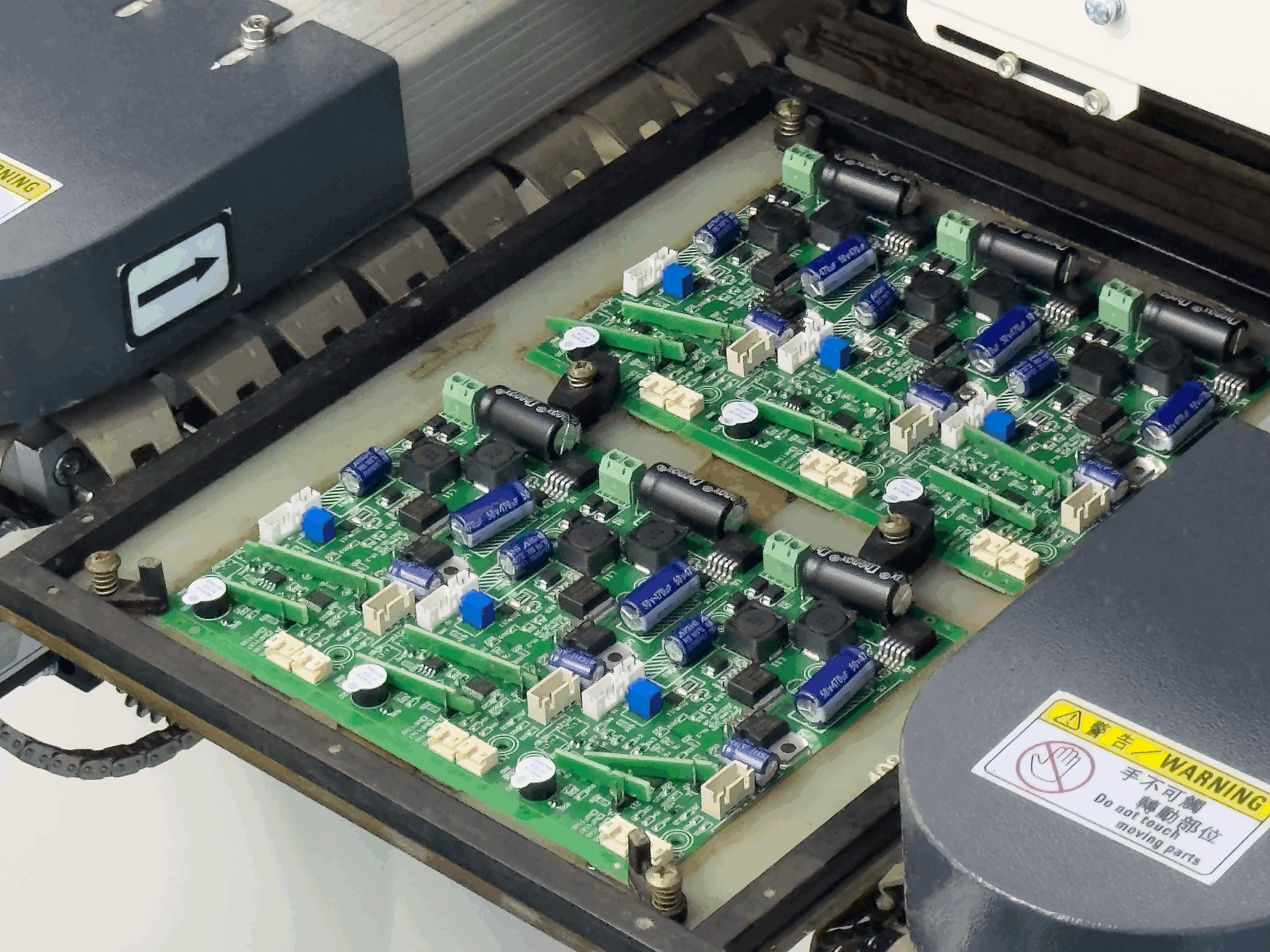
Thickness and Fine Features
The thickness sets the resolution that the mask can hold. A thick film flows and sags during the bake, so a narrow strip between two pads will close up before a thin one does.
The sidewall of a mask opening is a slope rather than a vertical face, and the slope becomes steeper as the film gets thicker. A steep sidewall is what allows a narrow dam between pads to survive, and it is also what makes the film crack at the base of the slope.
For a fine pitch part the usual answer is a thinner film, which is why a photoimageable mask is preferred over a screen printed one for a dense board. The thinner film holds the dam and gives a more predictable opening.
For a board that carries a fine pitch device, the mask thickness and the pad geometry should be checked together with the assembly house before the stencil is ordered, because the three features set the solder volume and the bridging risk at the same time.
The thickness also affects the appearance of the board. A very thin mask shows the copper texture through it, while a thick one hides the traces and can look uneven over a wide pour.
Adhesion and Cure
The adhesion of the mask depends on the surface preparation more than on the thickness. A copper surface that has been oxidised or contaminated before the mask is applied will lift at the edges, however thick the film is.
The cure has two stages: a prebake that removes the solvent and a final cure that cross links the polymer. An incomplete final cure leaves a film that is soft, that absorbs chemistry and that fails the adhesion test.
Over curing is also a problem, because a film that is baked too long becomes brittle and cracks at a sharp copper edge. The window between the two is narrower than the tolerance of a typical oven, so the cure profile has to be controlled.
The adhesion test is a tape pull on a test pattern and a cross hatch cut on a coupon. The solderability and adhesion tests are usually run together on the same coupon.
Mask Over Vias and Pads
A mask that spans a via forms a tent, and the practice of leaving the film over the hole is called tenting. The rule that allows it is a question of thickness, hole size and registration, and it should be stated explicitly rather than left to the shop.
A tent survives only if the film is thick enough to bridge the hole and thin enough not to sag into it, and the window between the two narrows as the hole gets larger.
A mask that spans a via forms a tent, and whether the tent survives depends on the via size and on the thickness of the film. A thick film bridges a larger hole, but it also sags more in the middle.
A mask that covers a pad leaves a surface that cannot be soldered, which is sometimes wanted and often a mistake. A pad that is covered by a mask cannot be probed, and the error is found only when the test fixture is built.
The mask also interacts with the surface finish, because the finish is applied after the mask in some processes and before it in others. The order decides whether the finish covers the mask or the mask covers the finish, and it is a question for the shop.
The etching process that formed the copper also set the edge profile that the mask has to cover, so a board with undercut traces is harder to coat than one with square edges.

Design Review
The review starts with the thickness and the tolerance, stated on the fabrication drawing. A note that names the material and the colour but not the thickness leaves the process engineer to choose, and the choice will be whatever the line runs most often.
The second item is the resolution that the board needs, checked against the thickness and the material. A fine pitch part on a thick screen printed mask is a combination that will not work.
The third item is the cure and the adhesion test, which should be specified for the first article and for any change of material. The laminate properties matter here, because a rough laminate holds the mask better than a very smooth one.
The last item is the appearance of the finished board, checked against the sample that the customer approved. The quality judgement on a coated board is made partly by eye, and the standard should be written down rather than remembered.
FAQ
How thick is solder mask normally? Typically between fifteen and thirty microns over the copper, with the value depending on the material and the method. The thickness over a trace is higher than the thickness on the laminate.
Can solder mask be too thick? Yes. A thick film sags between fine pads, cracks at sharp copper edges and can close a narrow dam, so a dense board usually needs a thinner film.
Why does the mask lift after soldering? Usually because the surface was contaminated or the cure was incomplete. Both show up as a lift at the edge of a pad, and both are process issues rather than artwork issues.