Backdrilling: Design Rules and Process Limits
A plated through hole that connects an inner layer to the outside is drilled through the whole board, so the part of the barrel below the layer that matters is a length of copper that carries no signal. That unused length is the via stub, and at high frequency it behaves as a transmission line with an open end. The reflection and the resonance it produces are among the largest contributors to loss on a long channel.
This article explains what the stub does electrically, when it becomes significant, how it is removed by backdrilling, how the depth is controlled, and what the design can do to reduce the need.
What A Via Stub Is
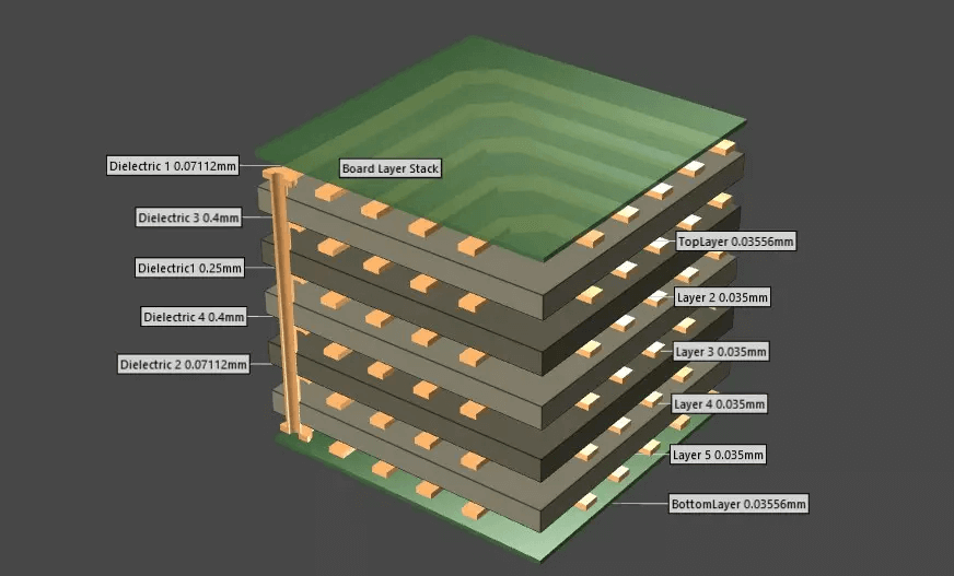
The barrel of a through via runs from the top of the board to the bottom, regardless of which layers it has to connect. If a signal enters on layer one and leaves on layer four of a twenty layer board, the sixteen layers below are a stub. The stub is a length of copper open at one end, so any signal travelling along the via reflects from that end and returns, arriving later than the direct signal and adding to it.
The result is frequency dependent. At low frequencies the delay of the reflection is a small fraction of the rise time and the stub is invisible. At high frequencies the reflected signal arrives out of phase and cancels part of the transmitted one, and at the frequency where the stub is a quarter of a wavelength the cancellation becomes a deep notch that no amount of equalisation can restore.

When Stubs Matter
The rule of thumb is that a stub starts to be a problem when its electrical length exceeds about one tenth of the rise time of the signal, which for a 25 gigabit per second channel is a stub of a few tenths of a millimetre. On ordinary boards with signals of a few hundred megahertz, a stub on a two millimetre thick board is harmless, and backdrilling would be an unnecessary cost.
The calculation changes with the board thickness and with the layer the signal uses. A signal that enters on layer one of a thick backplane has a long stub and suffers; the same signal in the middle of a thin board has almost none. That is why backdrilling is common on backplanes, on line cards and on any board that carries a long serial channel to an external connector.
The Backdrilling Process
Backdrilling is a controlled drilling operation performed after plating. A drill of a larger diameter than the via is driven into the barrel from the side opposite the connection, removing the unwanted copper. The operation is normally done with a machine that registers on the same data as the original drilling and measures the depth, because the target is a specific distance from the pad rather than a specific depth from the surface.
Two consequences follow from using a larger drill. The first is that the drill removes the pad on the layers it passes through, so no other net may use those layers at that position, and the design has to reserve the area around the via. The second is that the drill leaves a small tapered cavity, which has to be clear of the layers the via still connects and which is measured as the remaining stub length.
Depth Control And Tolerance
The remaining stub is what the process controls, typically between 0.2 and 0.4 millimetres from the layer that the via must reach. The tolerance has to allow for the drill depth accuracy, for the thickness of the plated copper, for the position of the layer within the board and for the drill wear, and it is therefore stated as a maximum, not a nominal.
The alternative to backdrilling is to avoid the stub by construction. A blind via reaches only the layers it connects and a buried via connects only inner layers, so neither has a stub. The choice between them and a backdrilled through via is a stackup decision as well as a cost decision, and the options are described under blind and buried via stack selection.
Design Choices That Reduce The Need
The simplest way to reduce a stub is to route the signal on a layer close to the surface where the connection is made. A signal that enters on layer one and leaves on layer three has a shorter stub than one that leaves on layer ten, and a layout that keeps high speed routing near the outer layers reduces the number of vias that need backdrilling.
The second choice is to use a via whose connection is made at the last inner layer, so that the stub is the thickness of the outer laminate only. Neither option is always available on a dense board, and both have to be balanced against the crosstalk and the layer assignment that the rest of the design needs. The transmission line structures that the vias sit between are described under microstrip and stripline routing, and the stack that results is discussed under layer stackup from one to eight layers.
Verification
The stub is verified by a coupon that is sectioned and measured, and by a measurement of the channel itself. A coupon with a via of the production geometry, backdrilled with the production parameters and sectioned, shows the remaining stub length and the condition of the copper at the bottom of the hole. The section is the only method that shows whether the drill went too deep.
The electrical verification is a measurement of the insertion loss of a channel that contains a backdrilled via, compared with the same channel without the stub. The improvement in the notch is the evidence that the process is working, and it is normally recorded as part of the qualification of a high speed product rather than checked on every lot. A design that relies on backdrilling and has no coupon to prove it is relying on the fabricator’s process control alone.
Where It Fits In The Signal Integrity Flow
Backdrilling is a late answer to a problem that is better addressed early. A signal integrity simulation that includes the via model will show the notch in the channel response, and the engineer can then choose between a thinner board, a different layer assignment, a blind via or a backdrilled through via. The cost of each is known at that point, and the choice is made with the whole channel in view rather than by adding a process step after the layout is frozen.
A simulation that models the via as a simple inductance, however, will miss the effect entirely, because the reflection is a transmission line phenomenon rather than a lumped one. The via has to be represented as a length of line with an open end, and the model has to use the actual stub length from the stackup. When that is done, the effect is visible in the simulated eye diagram long before it is measured on a board.
FAQ
Does backdrilling damage the via? It does not, provided the drill stops above the layer the via must reach. The risk is a drill that goes too deep and removes copper from a layer that the signal needs, which is an open circuit rather than a damaged barrel.
Can any via be backdrilled? Only if the layers between the surface and the drill path carry nothing that uses that position. The design has to keep a clearance zone around the via that the larger drill will enter.
Is backdrilling needed on a differential pair? Only if the stub is long enough to affect the channel. On a thick backplane it is often required, while on a short link on a thin board the stubs are small enough to be ignored.