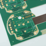
USB Routing and Impedance Requirements for Reliable Links
USB is designed to be robust, and that robustness hides a great deal of layout sloppiness at low speed. At the current data rates, however, a poorly routed pair produces intermittent enumeration, failed transfers and devices that work on one cable and not another. The rules that prevent that are simple, and they are mostly about impedance and continuity.
Why USB Routing Rules Exist
The interface carries a differential signal whose quality determines whether the receiver can recover the data. Reflections, skew and common mode noise all reduce the margin, and each of them is produced by a specific layout mistake. The rules exist because those mistakes are easy to make and hard to diagnose afterwards.
The symptom of a marginal link is rarely a total failure. It is a device that negotiates at a lower speed than expected, a transfer that retries, or a port that works with one host and not another. Those behaviours are the reason the layout has to be verified by measurement rather than by hoping.
Data Rates and Their Requirements
Each generation of the interface raises the demands on the layout. Low and full speed are tolerant of almost any routing. High speed demands controlled differential impedance and a solid reference plane. The faster generations demand tighter impedance control, shorter stubs and better return path management.
The connector and the cable are part of the channel, and their contribution grows as the data rate rises. A board that is perfect up to the connector can still fail if the connector footprint is poorly laid out, which is why the launch into the connector deserves the same care as the trace.
<img src="https://www.gopcba.com/wp-content/uploads/2023/05/2.jpg" alt="USB connector footprint with a differential pair routed to the pins” />
Differential Impedance and Stack-Up
The pair must present the impedance the standard requires, within its tolerance, across the whole route. That means the stack-up has to be designed so the required width and gap are achievable with the fabrication process, and the impedance has to be verified on a coupon rather than assumed.
Changes in geometry along the route change the impedance. A pair that widens to pass between connector pins, or that narrows to squeeze past a via field, presents a discontinuity at each change. Where the geometry must change, the change should be gradual rather than abrupt.
Routing the Pair Through the Connector
The traces must reach the connector pins with a controlled impedance and a short, symmetrical fan out. Pins on the connector are at a fixed pitch, so the pair has to spread to meet them, and that spreading is itself a discontinuity that should be kept as short as possible.
Ground pins adjacent to the signal pins provide the return path, and they should be connected to the reference plane with short vias. A connector whose ground pins are connected only at the far end of the board forces the return current to travel, which degrades the signal and radiates at the same time.
Length Matching and Skew
The two traces of the pair should be matched closely, because skew converts differential signal into common mode noise and reduces the eye opening. The tolerance depends on the data rate, and it is normally stated in the interface specification along with the impedance requirement.
Length compensation should be applied where the mismatch occurs. A pair that is matched at the connector but mismatched at the transceiver still carries the skew for the length between them, because the correction is at the wrong end of the error.
Power, Ground and Charging Paths
The power conductors carry current for charging as well as for signalling, and at high charging rates that current is significant. The power and ground traces should be sized for the current with an acceptable temperature rise, and they should be kept away from the signal pair to avoid coupling.
Bulk capacitance near the connector helps to supply transient current during enumeration and during load steps. Its placement should minimise the loop between the capacitor, the connector and the ground return, in the same way as any other power delivery network, following the same component tolerance and reliability logic used for the rest of the assembly.
Shielding, ESD and Protection Placement
ESD protection must be placed so that the transient current does not pass through the signal path before it is diverted. That means the protection device should be close to the connector, with a short, wide path to ground, and the protected node should be the connector side of the device.
The connector shell and any shield should be tied to ground with a low impedance connection, often through a small capacitor or a ferrite in applications where the shield is also a chassis connection. The choice affects both emissions and immunity, and it should follow the system grounding approach rather than being decided locally.
Connector and Cable Considerations
Connectors differ in their high frequency performance, and a part intended for charging only may not support the fastest data rates. The footprint, the pin arrangement and the internal structure all matter, and the manufacturer’s data should be checked against the required data rate.
Cables are equally variable. A cable that does not meet the impedance or loss requirement for the speed will fail regardless of the board, and field complaints about a product that works with one cable and not another are usually a cable quality issue rather than a design issue.
Verification and Compliance
Verification starts with the impedance coupon, which confirms the stack-up produces the required differential impedance with the production geometry. The next step is a measurement of the assembled channel, using an eye diagram or a compliance test fixture, which captures the effect of the connector and the launch.
Compliance testing is required for products that carry the certification mark, and it exercises the link under a defined set of conditions. Failing a compliance test at the margin is usually traceable to a specific layout feature, and the trace and connector structures involved are described in this guide to high speed design rules.
Process Control and Verification
On a design of this kind, impedance is the item that decides how the rest of the board is arranged. The measurements that matter are the repeatable ones: conductor width and spacing, annular ring, finished hole size, plating thickness and surface finish are all verifiable on a coupon that travels with the panel. Running a first article through the same checks as the production panel confirms that the two agree, and that comparison is the cheapest form of process control available at prototype stage.
FAQ
Does USB routing matter at low speed? Much less. Low and full speed links tolerate wide impedance variation and long stubs, which is why a board can pass at those rates and fail when a high speed device is connected to the same port. Design for the fastest device the port will ever see.
How closely must the pair be matched? The requirement comes from the interface specification and becomes tighter with each generation. Matching to a small fraction of a millimetre is typical for the fastest links, while earlier generations tolerate considerably more.
Why does my device fail to enumerate? Common layout causes are a broken or discontinuous reference plane, a large stub at the connector, an impedance that is out of tolerance, and ESD protection placed after the branch to the transceiver. Each of these degrades the signal enough to prevent negotiation.