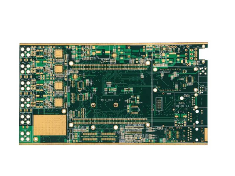
Solder Mask Dam Design Between Fine Pitch Pads
A solder mask dam is the narrow strip of mask that separates two adjacent pads. Its purpose is to stop molten solder from wicking from one pad to the next during reflow, and its width is one of the tightest features on a modern board.
As pitch falls the dam becomes narrower and the tolerance on its position becomes critical. A dam that is too thin, or one that has moved because of registration error, lets solder cross from one pad to the other and produces a bridge.
What The Dam Does
During reflow the solder is liquid and it will flow along any continuous copper path it can wet. The mask dam interrupts that path by providing a surface the solder cannot wet, so each joint stays contained within its own pad and mask opening.
The dam also protects the laminate between the pads and reduces the chance of surface contamination bridging them. On a high voltage design it contributes to the creepage distance, although it should never be the only insulation that the design relies upon.
Width Rules For Fine Pitch
A practical minimum dam width is about 0.1 mm, and 0.075 mm is achievable with a well controlled process. Below that the mask is difficult to develop cleanly and tends to lift during subsequent processing or during assembly.
The dam width follows from the pitch minus the mask opening, divided by two for the usual two sided case. At a 0.4 mm pitch with a 0.25 mm opening the dam is 0.075 mm, which sits at the limit of a standard process and pushes the design into a tighter class. The pad geometry it depends on is described under PCB pad design standards.
Registration And Mask Movement
Registration of the solder mask to the copper is as important as the dam width itself. If the mask shifts to one side, one dam grows and the other shrinks, and the narrow one may disappear completely.

The registration tolerance for a fine pitch design is typically plus or minus 0.05 mm, and it has to be added into the dam width calculation rather than assumed. A nominal dam of 0.1 mm with a 0.05 mm shift can vanish entirely. The ink behaviour behind this is described under solder mask ink thixotropy.
Wicking And Bridging
Wicking is the movement of solder along a surface by capillary action. It is driven by the surface energy of the molten alloy and by the geometry of the gap, and it becomes easier as the gap narrows and as the mask layer becomes thinner.
A bridge forms when the wicking reaches the neighbouring pad and the two joints become one. On a fine pitch component a bridge can connect dozens of pins, and rework is difficult because the solder has to be removed without disturbing the adjacent joints.
When To Remove The Dam
Some designs deliberately remove the dam and use a single mask opening across a row of pads. This is done on a fine pitch connector where the dam cannot be manufactured reliably, and it relies on the stencil aperture and the paste volume to control the solder instead.
Removing the dam is a trade. It eliminates the risk of a missing dam and the defects that follow, but it also removes a barrier that was helping to contain the solder. The decision should be supported by a paste volume analysis rather than taken as a default.
Inspection And Process Control
Inspection of the dam is partly visual and partly dimensional. A visual check looks for missing sections, lifted edges and mask residue inside the opening, while a measurement on a cross section gives the actual width in the finished product.
Process control on the mask side covers the exposure dose, the development time and the curing schedule, all of which affect the edge quality of the dam. How the mask requirement is documented is described under PCB design and fabrication.
Paste Volume And The Dam
The dam is only one of the controls on bridging. Paste volume, pad geometry and the reflow profile all contribute, and reducing the volume is often more effective than widening the dam. A deposit that is 20 percent too large will bridge across a dam that is perfectly made.
The stencil aperture should be designed together with the mask opening rather than separately. Aperture size, mask opening and dam width form a single set of dimensions, and optimising one without the others usually moves the problem rather than solving it.
Second Side Reflow And Mask Condition
A board that is reflowed twice sees the mask at temperature twice. Mask that was only marginally cured can soften on the second pass, and a softened dam no longer holds the solder back. The cure schedule should be set for the worst case, which is the second reflow.
Mask adhesion is also tested by the reflow itself. A dam that lifts during the second pass exposes bare laminate between the pads, and solder can then bridge across the exposed surface even though the dam was present at the first inspection.

Mask Thickness And Its Limits
The height of the dam depends on the mask thickness, which is typically 15 to 25 microns over the copper. A dam that is thinner than the pad opening is easier to develop but provides less of a barrier to solder that is already flowing.
On a fine pitch design the dam is usually the same thickness as the rest of the mask, and the limiting factor is resolution rather than height. Increasing the thickness to improve the barrier would close the openings, so the two requirements have to be balanced.
Working With The Fabricator
The achievable dam width is a process capability, and it should be confirmed with the fabricator rather than assumed from a data sheet. A supplier who holds 0.1 mm reliably may only manage 0.08 mm on a particular panel size or copper weight.
Where the design sits at the limit, it is worth adding a note to the drawing that identifies the critical dam locations. That allows the fabricator to concentrate inspection where it matters instead of measuring every dam on the panel.
Rework And Repair
A dam that is damaged during rework cannot easily be restored. Once the mask between two pads has been scraped away, the solder has a continuous surface to flow along, and the bridge is likely to return at the next reflow. The board should be reworked with that limitation in mind, and the area re-inspected afterwards.
Where rework is frequent, the mask dam is better treated as a consumable part of the process than as a permanent feature. Some production lines keep a dispensed mask resin on hand to rebuild the dam after rework, and that practice is common on high value assemblies where scrapping the board is not an option.
FAQ
What is the minimum solder mask dam width? Around 0.1 mm is a safe practical minimum, and 0.075 mm is achievable with a tightly controlled process. Anything narrower needs a capable supplier and a tolerance study.
Does a wider opening always risk a bridge? Not by itself. Bridging depends on the paste volume, the pad geometry and the profile as well as on the mask. The dam removes one route, it does not remove the cause.
Should the dam be removed for a fine pitch connector? It is sometimes the better choice when the dam cannot be produced reliably. The decision should be based on measured process capability rather than on preference.