Gold Embrittlement in Solder Joints: Thickness Limits and Control
Gold is a finish that protects a surface before assembly and then becomes a liability during it. Dissolved into molten alloy it forms hard intermetallic plates that sit exactly where the joint carries its highest strain, and the resulting failure appears months later as a fatigue crack at the pad interface. This article covers the dissolution mechanism, the thickness limit that keeps it under control, and the measurements that tell a process engineer whether a delivery of boards can be soldered as it stands.
How Gold Enters the Joint
Gold dissolves in molten tin-lead and in lead-free alloys at a rate that depends on temperature and time, and the dissolved gold forms intermetallic compounds that appear as needle-like plates in the joint. The compound is hard and brittle, and it concentrates at the interface where the joint sees the highest strain during thermal cycling.
The dissolution is fast. A one micrometre gold layer is consumed within a few seconds at 250 degrees Celsius, and the gold concentration that results in a typical joint can exceed three percent by weight, which is already past the point where the mechanical properties change.
The Four Percent Rule and Where It Comes From
The widely quoted limit is that the gold content of a solder joint should stay below about four percent by weight, and that figure is a practical threshold rather than a sharp transition. Above it the joint loses ductility quickly, while below it the intermetallic still forms but the plates remain small and dispersed.
The rule translates into a plating budget: gold thickness multiplied by plated area, divided by joint volume, gives the concentration. That is why a thick gold layer on a small joint is far more dangerous than the same thickness on a large one, and why the calculation belongs in the design review rather than being left to the shop.
The calculation is quick and worth doing on any connector or pin that will be soldered, because the joint volume is set by the pad and the paste print and cannot be increased later.
Where Thick Gold Appears
Hard gold on edge connectors is normally 0.8 to 1.5 micrometres over nickel and is never soldered, so it is not the problem. The risk comes from gold plating used as a solderable finish, from gold-plated pins and pads that will be soldered, and from gold flashed components assembled with the same profile as the rest of the board.
Nickel under the gold is the barrier that limits dissolution, because tin does not dissolve nickel at anything like the gold rate. A nickel layer of 3 to 6 micrometres between the copper and the gold reduces the amount of gold exposed to the alloy, and where gold is unavoidable that barrier thickness is the variable to specify.
Process Variables That Worsen It
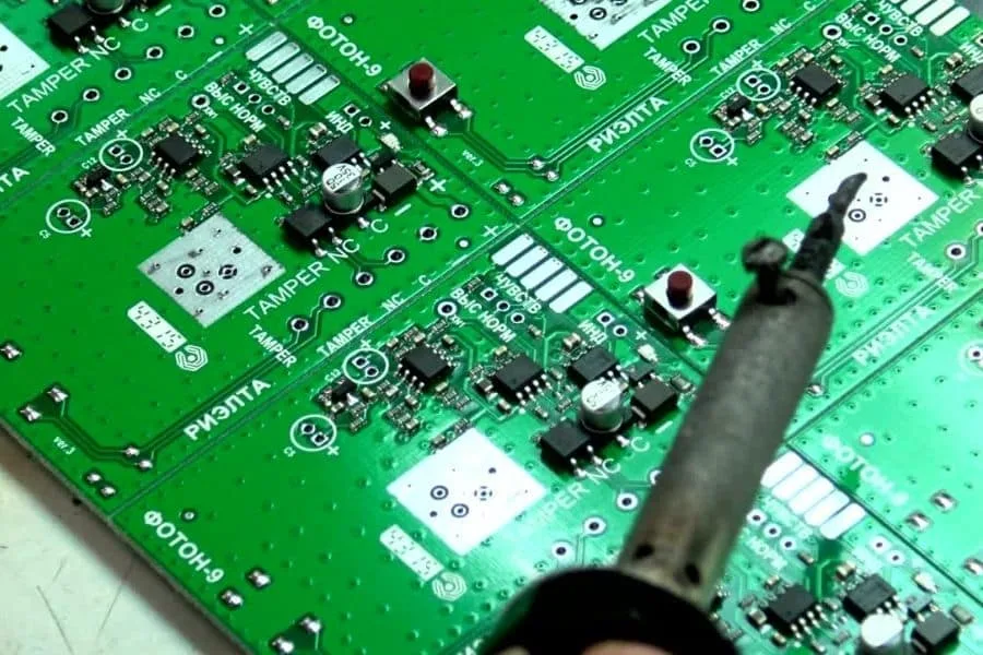
Iron temperature and contact time are the two variables that decide how much gold dissolves during hand soldering. An iron at 400 degrees left on a gold-plated pad for five seconds dissolves far more gold than one at 320 degrees for two seconds, and the difference in joint quality is visible in a microsection.
In reflow the same logic applies to time above liquidus rather than to iron contact, and a profile with a long liquidus dwell dissolves more gold than a short one. Where gold-plated surfaces must be reflowed, the profile is shortened and the peak is kept at the low end of the paste window.
Failures That Follow
Gold embrittlement fails in fatigue rather than in a single overload. The crack runs along the intermetallic layer at the interface, it grows with every thermal cycle, and the joint resistance rises gradually until the connection becomes intermittent rather than open.
The failure is difficult to attribute, because the joint looks acceptable at inspection and the contamination is invisible without a section. A field return that shows a crack at the pad interface with a gold-tinted compound along it is the signature, and it usually appears on boards built from the older plating batch.
Detection and Measurement
Microsection with energy dispersive X-ray analysis is the method that quantifies the problem, because it shows both the intermetallic distribution and the elemental composition at the interface. Scanning electron microscopy alone shows the plate structure but not the concentration.
For production control the practical test is a plating thickness measurement on incoming boards using X-ray fluorescence, checked against the thickness on the drawing. If the finish is thicker than specified, either the gold is removed before assembly or the boards are returned, because the joint cannot be made acceptable by adjusting the profile alone. Our plating thickness notes describe the measurement.
Removing Gold Before Soldering
Where a delivery has arrived with too much gold, the standard remedy is to wick it off before assembly: flux the pad, apply solder with an iron or hot air, and remove the alloy with braid so that most of the gold leaves with the first wetting. Two passes typically reduce the residual gold to a level the joint can tolerate.
The method has limits. It works on accessible pads and pins, it consumes time in proportion to the number of joints, and it risks damaging the pad if the iron is too hot or the braid is held too long. On a fine pitch device, the same result is better achieved by specifying a thinner gold in the first place.

Wicking changes the pad surface as well as removing gold, so the solderability of the pad has to be re-checked before the component is placed, particularly where the finish was the only protection against oxide.
Specifying the Finish on the Drawing
The drawing should state the gold thickness and its tolerance, the nickel barrier thickness beneath it, and the basis of the measurement, whether that is X-ray fluorescence on the surface or a microsection from a coupon. A note that says simply hard gold leaves the thickness to the fabricator.
Where gold is required for wear on an edge connector, the note should also state that the gold is not to be soldered and that the solderable areas carry a different finish. Mixed finishes on one board are common, and they cause trouble only when the drawing does not distinguish the two areas.
Process Control After the Change
Once the thickness is specified, the control loop is a receiving inspection measurement on every delivery, recorded against the batch. The measurement is quick, it needs no destructive preparation, and it is the only way to know whether a supplier has changed its process between shipments.
The other half of the control is the profile used for gold-bearing assemblies. If the same profile runs whether gold is present or not, the operator has no way to know that a shorter liquidus dwell applies, so the profile gets a separate entry in the machine programme with the surface finish noted beside it. Joint acceptance criteria for the result are set out in our acceptance criteria guide.
FAQ
Does gold embrittlement affect lead-free solder too? Yes. Gold dissolves in tin-based lead-free alloys as well and the intermetallic that forms is equally brittle, so the four percent guidance applies to both systems.
Is immersion gold the same as hard gold? No. Immersion gold is a thin porous layer over nickel intended to protect the nickel during storage, with a thickness of a fraction of a micrometre, so it is not a source of embrittlement.
Can a gold contaminated joint be reworked? Removing the joint and the gold beneath it and rebuilding the surface is the only reliable repair, because reheating the joint redistributes the intermetallic rather than removing it.