PCB Test Point Design: 7 Rules for Reliable ICT Access
A PCB test point design decides whether the assembly can be probed at all, and it is a small piece of layout work with a large effect on test cost. A board that cannot be reached needs a fixture change, a flying probe program or a redesign, and all three cost far more than the copper a test pad would have used.
Test points are usually added late, once the layout is tight and the test engineer asks for space. That is the wrong order, because the correction is cheap only while the layout is still open. The rules below apply to in circuit test, flying probe and functional test alike, and their purpose is to keep ICT access open.
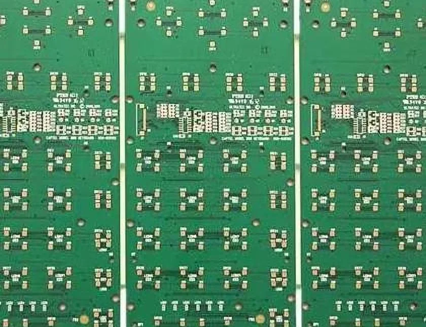
<img src="https://www.gopcba.com/wp-content/uploads/2026/05/smart-energy-PCBA.jpg" alt="PCB test point design with probe access on an in circuit test fixture” />
What a Test Point Has to Provide
A test point has to give a probe a stable contact with low resistance, and it has to do so thousands of times without wearing the surface away. That means exposed metal, a flat surface and enough area for the probe tip to land inside the pad even when the fixture is slightly off centre.
A test point is not a pad that happens to be free. It is a defined feature with a size, a position and a keep out area around it, and it should be entered in the netlist as such so that it survives later layout edits and a re layout of the board. That entry is what turns a free pad into a documented test point.
Pad Size and Probe Geometry
The test pad must be larger than the probe tip by a comfortable margin. A typical spring probe has a tip of a fraction of a millimetre, but placement tolerance in the fixture is far larger than that, so a pad near one millimetre across is a common working minimum.
Square pads give more usable area than round pads of the same width, which matters on a dense board. Where the probe is a crown or a serrated tip, the pad should be large enough that the scoring stays inside the metal rather than cutting the solder mask edge. The pad should also be free of any via in pad construction that would leave its surface uneven.
The Test Grid and Spacing
A bed of nails fixture is built on a fixed grid, usually 1.27 mm or 2.54 mm, and test points that ignore that grid cannot be probed by a standard fixture at all. Placing every test point on the grid turns a custom fixture into a catalogue item and cuts both cost and lead time.
Spacing matters as much as position. Two test points closer than the probe body allows will interfere mechanically, so the clearance is set by the probe housing rather than by the copper. The practice described in ICT fixture probe maintenance shows how that clearance is checked.
Solder Mask and Surface Finish
A test point must be free of solder mask, because a probe cannot penetrate a cured film reliably. The mask opening should be defined in the same layer as the pad so that the two cannot drift apart, and the opening should be slightly larger than the pad to allow for registration.
Surface finish matters too. A hard, flat finish such as thin gold over nickel gives a stable contact resistance over many touchdowns, while a thick solder finish deforms under the probe and builds up oxide that raises the resistance of every later measurement. Mask thickness at the opening matters as well, because a thick film forms a step the probe has to cross.
Using Vias and Existing Pads
A via can serve as a test point if it is untented and the barrel is open, but a via in a dense area may be too small or too close to its neighbours. Untented vias are a cheap source of extra probe access on boards where dedicated pads will not fit.
Connector pins and component pads should not be used as test points unless there is no alternative. A probe on a fine pitch lead can bridge two pins or damage the joint, and the risk grows as the pitch shrinks and the leads become more fragile.
Test Points and Signal Integrity
A test point adds a stub to the net, and on a fast signal that stub is a reflection point. The effect is small at low frequency and significant at high frequency, so a test point on a high speed net should be short and placed near the driver rather than at the far end of the trace.
Where a net cannot tolerate a stub, the test access may have to be a via on the trace itself or a boundary scan path. The coverage question is discussed in design for test coverage analysis work, which weighs reachable nets against the cost of probing them.
Test Point Design Rules That Keep Coverage
Test points should be placed on a regular grid, kept clear of tall components, and grouped so that the fixture can support them. A test point under a tall capacitor is unreachable in practice, and one at the very edge of the board may fall outside the fixture frame.
Component height is the usual reason a designed test point cannot be used. The rule is to keep a defined height envelope above every test point, and the same review that checks assembly clearance should check the probe side. The agenda used in assembly DFM review covers this as a standing item. The same envelope applies to the probe side of the fixture, where the probe body needs its own clearance.
Coverage Measurement
Coverage is the share of nets that a given test method can reach, and it should be measured rather than assumed. A report listing reachable nets, probed nets and nets left to functional test turns a vague claim into a number that a project can act on.
A common target is to probe the large majority of nets, with the remainder covered by boundary scan or functional test. Where coverage is short, the cheapest fix is usually one more test point on a net that is already routed near the probe side of the board.
Records and Change Control
The test point list, the netlist revision and the fixture revision should be kept together, because a change to any one of them can invalidate the others. A re layout that moves a test point by a millimetre is invisible on a schematic and fatal to a fixture.
Where the product follows a published standard, such as the testability guidance from IPC, that reference belongs in the design rule document so the rules survive a change of engineer. PCB design review and functional test fixture design cover the stages either side of this one.

FAQ
How large should a test point be? Large enough for the probe tip plus the placement tolerance of the fixture, which usually works out near one millimetre on a standard grid. Square pads give more usable area than round ones.
Can a via be used as a test point? Yes, if it is untented and the barrel is open, but a via that is small or crowded may not accept a probe reliably. Dedicated pads are better where the board has room.
Why does test coverage fall after a layout change? Because a moved test point can leave the fixture grid or end up under a tall component. The test point list has to be re checked against the new layout before the fixture is ordered.