
Hot Air Solder Leveling Thickness Control
Hot air solder leveling covers the exposed copper with a thin solder coating and then blows the excess off with heated air, and the thickness it leaves behind is set by the balance between the two. A coating that is too thick bridges fine pitch features, while one that is too thin leaves copper exposed and the finish fails its solderability requirement.
The process is one of the few in PCB fabrication that relies on a controlled amount of imperfection, because a coating of even thickness across every feature is not achievable. The practical aim is a distribution whose minimum still protects the copper.
What Hot Air Solder Leveling Does
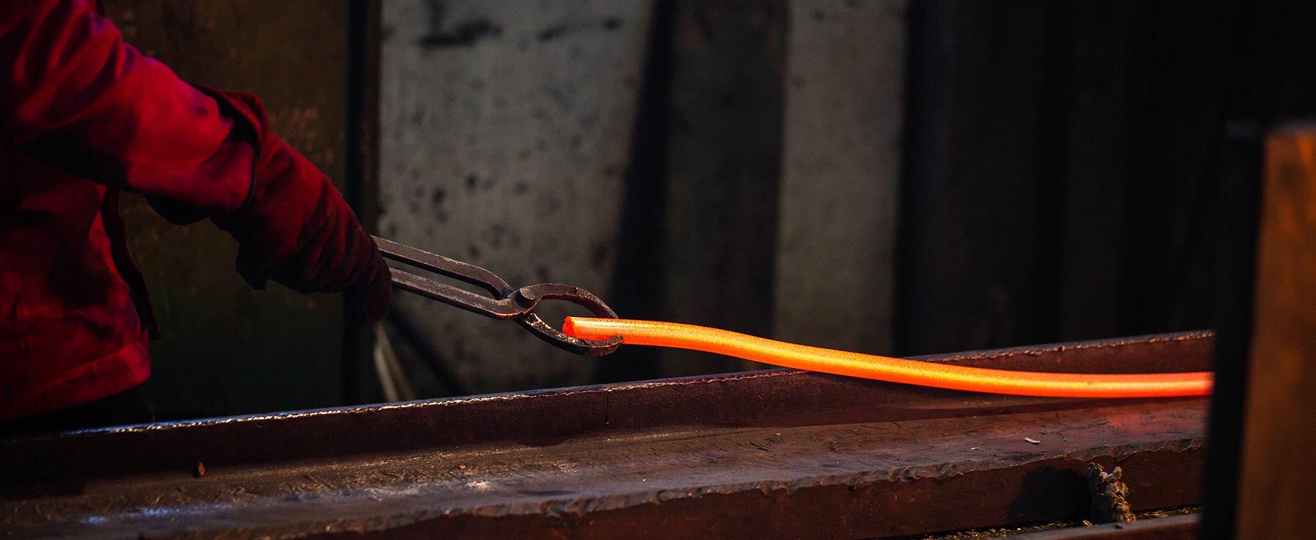
Boards are fluxed, dipped into molten solder and withdrawn through air knives that shear the surplus away. The remaining coating protects the copper and provides a solderable surface, and it is consumed into the joint during assembly.
Coating takes place after solder mask, so the mask and the coating see each other. A mask that has not fully cured will be damaged by the thermal excursion of the solder bath, and the damage appears as a lifted mask edge after leveling. The coating is a solder alloy rather than a plated metal, so it melts in the reflow oven and becomes part of the joint instead of remaining a surface layer.
Coating Weight and Measurement
Coating is specified as a weight per unit area or as a thickness, and the two are related by the density of the alloy. Typical requirements sit between 1 and 2 micrometres on the surface and between 5 and 25 micrometres in the hole.
The measurement is made by a beta backscatter gauge on a pad, by an X-ray fluorescence instrument or by microsection of a plated hole. The methods read different things, so the acceptance criterion should name the method that will be used for the decision. The HASL thickness on a fine pitch pad is the value that matters most at assembly, because the excess solder there is what bridges neighbouring pads.
Air Knife Settings and Uniformity
The air knives are the primary control on thickness. Pressure, temperature, the gap between the knives and the angle at which they meet the board all change how much solder is removed, and the settings interact strongly with the withdrawal speed.
Uniformity across the panel depends on the knives being aligned to the board rather than to the machine frame. A knife that is slightly out of parallel removes more solder on one side, and the difference shows on a thickness map as a gradient from one edge to the other. Air knife pressure is set as low as the coating allows, because higher pressure removes more solder but also disturbs the coating inside the holes.
Solder Bath Temperature and Alloy
The bath is held between 245 °C and 265 °C, and the alloy is normally tin-lead for a conventional finish or a lead-free tin-copper or tin-silver-copper alloy for a lead-free one. Copper content rises as boards pass through the bath, and the alloy should be analysed on a schedule.
The thermal excursion is significant for the laminate. Boards are in the bath for a few seconds, and the surface of the substrate reaches a temperature high enough to distort thin panels, which is one reason leveling is followed by a flattening or a pressing step. Withdrawal speed interacts with every other setting, and it is the parameter that is changed most often when a new panel size is introduced.
Flux Selection and Residue
Leveling flux has to survive the bath temperature and still be removable, and it is usually a water-soluble or a rosin-based chemistry with a high solids content. The residue it leaves is significant and must be cleaned as covered in the notes on leveling flux.
Residue that is not removed becomes a contamination source at assembly. It also affects the ionic cleanliness measurement, which is why cleaning verification follows leveling rather than preceding it. A bath that is low on tin or high on copper raises the melting range, and the coating then freezes earlier on the board and levels less evenly.
Thickness Effects on Assembly
A thick coating flows during reflow and can bridge between pads on a fine pitch footprint. The excess solder also changes the stand-off of a component, because the paste is joined by the coating on the pads and the hole walls.
A thin coating oxidises more quickly and can be consumed before the joint forms, particularly on a surface mount pad that sees only one reflow. Where the assembly uses a fine pitch part, the coating requirement is often tightened for that area alone, as discussed in the comparison of surface finishes. Flux residue also affects the appearance of the coating, and a board that looks dull after cleaning usually has a residue problem rather than a thickness problem.
Solderability and Aging
Solderability is measured by a wetting balance or a dip test, and the result depends on the coating thickness, the intermetallic layer beneath it and the storage conditions. A coating that passes the test on the day of manufacture can fail after six months in a humid store.
Coating thickness is one of the few parameters that can be adjusted after the fact, but the adjustment costs a second pass through the machine. The second pass adds another thermal excursion to the laminate, which is why the first pass should be controlled rather than corrected. Where the coating is too thin, the copper beneath it can oxidise during storage, and the oxide is not removed by the flux at assembly.
Defects and Their Signatures
Leveling leaves a characteristic set of defects. Icicles and spikes form where the air knives fail to shear the solder from a hole, solder balls sit on the mask where droplets have landed, and blocked holes appear where the coating has bridged the barrel.
Mask adhesion loss and copper peel problems also appear after leveling, when the thermal excursion has found a preparation fault, which connects the process to the wider question of copper peel strength.
Records and Acceptance Limits
Records should carry the alloy analysis, the bath temperature, the knife settings and the withdrawal speed, together with the thickness map for the sample board. gopcb keeps those values with the lot so a coating problem can be traced to a set-up.
Acceptance should state the minimum and maximum coating on the surface, the minimum in the hole, the measurement method and the positions measured. The minimum matters more than the average, because a coating that is thick on average but thin at one pad is a solderability failure waiting to be found. The minimum coating on the surface and in the hole should be recorded beside the maximum, because the two limits fail for different reasons.
FAQ
How thick is a hot air solder leveling coating? Between 1 and 2 micrometres on the surface and between 5 and 25 micrometres inside a plated hole, with the minimum value governing the acceptance decision.
What causes icicles after leveling? Air knife pressure, temperature or angle that is not matched to the hole size and the withdrawal speed, so the solder is not fully sheared from the barrel before it freezes.
Does leveling damage the laminate? The bath imposes a short but severe thermal excursion, so thin panels are levelled with a controlled withdrawal and followed by a flattening step where flatness is critical.