In modern electronics manufacturing, almost every electronic product depends on one essential component: the printed circuit board (PCB). A PCB provides the electrical and mechanical foundation that connects electronic components, distributes power, transmits signals, and enables a complete electronic system to operate reliably.
For beginners, understanding the PCB assembly process may initially seem complicated. The process involves miniature components, precise placement equipment, soldering technologies, automated inspection systems, and strict quality-control procedures. However, once the workflow is understood, PCB assembly becomes a systematic manufacturing process that transforms an electronic design into a functional product.
From consumer electronics and communication equipment to automotive electronics, medical devices, industrial automation, and aerospace systems, reliable PCB assembly is essential for product performance and long-term durability.
This guide explains the complete PCB assembly process step by step, covering SMT assembly, THT assembly, soldering, inspection, testing, rework, and best practices. It also explains how a professional PCB manufacturer such as Kingda can help customers move from PCB design and prototyping to PCB assembly and volume production.
Introduction to Printed Circuit Board (PCB) Assembly
What Is PCB Assembly?
PCB assembly, commonly abbreviated as PCBA (Printed Circuit Board Assembly), is the manufacturing process of attaching electronic components to a fabricated PCB and soldering them to create a functional electronic circuit.
A bare PCB typically contains copper traces, pads, vias, dielectric layers, and solder mask, but it cannot perform its intended electronic function until components are installed.
During PCB assembly, components such as:
- Resistors
- Capacitors
- Diodes
- Transistors
- Integrated circuits (ICs)
- Connectors
- Sensors
- Modules
- Switches
are mounted onto the PCB using technologies such as Surface Mount Technology (SMT) and Through-Hole Technology (THT).
A simple way to understand the difference is:
PCB fabrication creates the circuit board, while PCB assembly turns the board into a functional electronic product.
Modern PCB assembly services can combine automated component placement, solder paste printing, reflow soldering, selective soldering, wave soldering, automated optical inspection, X-ray inspection, and electrical testing to achieve consistent production quality.
Why Is the PCB Assembly Process Important?
The quality of the PCB assembly process directly affects the electrical performance, reliability, service life, and safety of the final electronic product.
Poor assembly can result in:
- Solder bridges
- Open circuits
- Cold solder joints
- Component misalignment
- Missing components
- Tombstoning
- Insufficient solder
- Excessive solder
- Component polarity errors
- Electrical shorts
For example, a small solder defect on a high-density BGA package may be invisible to the naked eye but can cause intermittent electrical failures. This is why professional manufacturers use multiple inspection and testing methods throughout the assembly process.
Different industries also have different PCB assembly requirements. Automotive electronics require high reliability and resistance to temperature and vibration. Medical electronics require strict quality management and traceability. Industrial equipment may require long operating life and environmental durability, while consumer electronics emphasize compact dimensions, production efficiency, and cost optimization.
Common PCB Assembly Terminology
Beginners should understand several important PCB assembly terms.
SMT (Surface Mount Technology): Components are mounted directly onto the surface of the PCB. SMT is widely used because it supports high component density and automated production.
THT (Through-Hole Technology): Component leads pass through holes in the PCB and are soldered to the opposite side. THT is commonly used for large components, connectors, transformers, and components requiring strong mechanical connections.
BOM (Bill of Materials): A complete list of components required to manufacture a PCBA, including part numbers, quantities, specifications, and approved manufacturers.
Gerber Files: Manufacturing data used to fabricate the PCB, including copper layers, solder mask, silkscreen, and other PCB information.
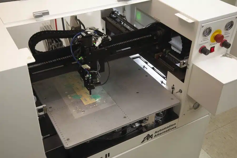
Pick-and-Place Machine: Automated equipment that accurately places SMT components onto PCB pads.
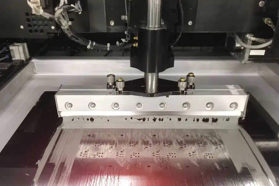
Stencil: A metal template used to apply solder paste accurately to the PCB pads.
SPI (Solder Paste Inspection): An inspection process used to measure solder paste volume, height, area, and position before component placement.
AOI (Automated Optical Inspection): A camera-based inspection technology used to identify component placement and soldering defects.
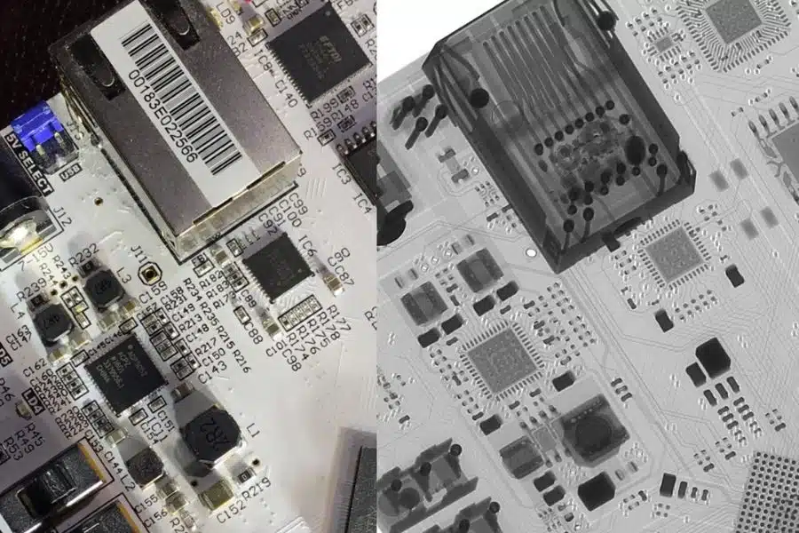
X-ray Inspection: A non-destructive inspection method used to detect hidden solder defects in BGA, QFN, CSP, and other packages that cannot be fully inspected optically.
Understanding these terms helps beginners communicate more effectively with PCB assembly manufacturers and identify potential production issues earlier.
Preparing for PCB Assembly
Before components are mounted, several preparation steps must be completed to ensure that the assembly process is stable and efficient.
Reviewing PCB Design Files
A successful PCB assembly process begins with accurate manufacturing data.
Typical files required for PCB assembly include:
- Gerber files
- BOM
- Pick-and-place files
- Assembly drawings
- PCB fabrication drawings
- Schematic diagrams
- Component specifications
- Special process instructions
The manufacturer should review these files before production to identify potential manufacturing problems.
A professional DFM (Design for Manufacturability) review can identify issues such as:
- Insufficient component spacing
- Incorrect pad dimensions
- Poor solder mask clearance
- Inadequate thermal relief
- Difficult component orientation
- Fine-pitch placement challenges
- Incorrect footprints
- Insufficient PCB-to-component clearance
Early DFM analysis can reduce rework, engineering changes, and production delays.
Component Sourcing and Inspection
Reliable components are equally important to reliable PCB assembly.
Manufacturers should verify:
- Manufacturer part number
- Component value
- Package type
- Polarity
- Date code where applicable
- Moisture sensitivity
- RoHS requirements
- Authenticity and supplier traceability
Counterfeit or incorrect components can cause serious reliability problems even when the PCB assembly process itself is properly controlled.
Professional PCBA suppliers should therefore maintain controlled component sourcing and incoming inspection procedures.
PCB Preparation
Before assembly, bare PCBs should be inspected for:
- Surface contamination
- Oxidation
- Scratches
- Damaged pads
- Warpage
- Solder mask defects
- Dimensional problems
Proper PCB storage is also important. Excessive moisture can negatively affect soldering performance and may increase the risk of delamination or other thermal-related defects.
Surface Mount Technology (SMT) Assembly
SMT assembly is the dominant technology used in modern electronic manufacturing because it supports high component density, miniaturization, and automated production.
A typical SMT workflow includes:
Solder Paste Printing → SPI → Pick and Place → Reflow Soldering → AOI → X-ray/Testing
1. Solder Paste Application
Solder paste printing is the first major stage of SMT assembly.
A stainless-steel stencil is aligned with the PCB, and solder paste is deposited onto the component pads using a squeegee.
The quality of solder paste printing depends on factors such as:
- Stencil thickness
- Aperture design
- Squeegee pressure
- Printing speed
- Paste viscosity
- PCB surface condition
- Environmental conditions
Too much solder paste may create solder bridges, while insufficient solder paste may result in weak or incomplete solder joints.
SPI Inspection
After printing, Solder Paste Inspection (SPI) can measure solder paste deposition and identify problems before components are placed.
SPI can detect:
- Insufficient solder paste
- Excessive solder paste
- Offset
- Missing paste
- Uneven deposition
- Printing defects
Detecting these problems early can significantly reduce downstream defects.
2. Component Placement
After solder paste printing, the PCB enters the pick-and-place process.
Automated placement machines accurately position SMT components onto their designated pads.
Modern PCB assembly may involve components ranging from relatively large connectors and power devices to extremely small passive components and fine-pitch IC packages.
Component placement accuracy is critical because even a small offset can affect solder joint formation.
Before placement, manufacturers should verify:
- Component orientation
- Reference designators
- Package type
- Polarity
- Feeder setup
- Component availability
- Placement coordinates
3. Reflow Soldering
After component placement, the PCB passes through a reflow oven.
The reflow process typically consists of several temperature zones:
- Preheating – Gradually increases PCB temperature.
- Soaking – Stabilizes thermal conditions and activates flux.
- Reflow – Raises the temperature sufficiently to melt the solder.
- Cooling – Solidifies the solder joints.
The exact temperature profile depends on the solder paste, PCB materials, component specifications, and assembly requirements.
A properly optimized reflow profile helps prevent:
- Cold solder joints
- Component damage
- Solder bridging
- Voids
- Warpage
- Insufficient wetting
For lead-free assembly, SAC-based solder alloys are widely used because of environmental and regulatory requirements.
4. Post-Reflow Inspection
After reflow, the assembled PCB undergoes inspection.
AOI Inspection
Automated Optical Inspection (AOI) uses cameras and software to identify visible assembly defects.
Typical AOI inspection items include:
- Missing components
- Incorrect components
- Component offset
- Polarity errors
- Solder bridges
- Insufficient solder
- Excessive solder
- Soldering defects
X-ray Inspection
For packages such as BGA, QFN, CSP, and other hidden-joint components, X-ray inspection provides additional visibility.
X-ray inspection can identify:
- Solder voids
- Hidden solder bridges
- Missing solder
- BGA misalignment
- Open solder joints
- Internal connection defects
For high-reliability applications, combining AOI, X-ray, and electrical testing provides a more comprehensive quality-control strategy.
Through-Hole Technology (THT) Assembly
Although SMT dominates modern electronics manufacturing, THT assembly remains important for many applications.
THT components have leads that pass through drilled holes in the PCB.
Typical THT components include:
- Large capacitors
- Transformers
- Power connectors
- Relays
- Switches
- Terminal blocks
- Mechanical components
Component Insertion
THT components can be inserted manually or automatically depending on the production volume and component characteristics.
Before insertion, operators should verify:
- Component value
- Reference designator
- Polarity
- Lead orientation
- Hole position
- Component height
Correct insertion prevents polarity errors and mechanical interference.
Wave Soldering
Wave soldering is commonly used for boards containing multiple THT components.
The PCB passes over a controlled wave of molten solder, allowing multiple component leads to be soldered simultaneously.
Advantages include:
- High production efficiency
- Consistent soldering
- Suitable for larger production volumes
- Reduced manual soldering
However, wave soldering requires careful PCB design and component selection.
Hand Soldering
Hand soldering remains useful for:
- Prototypes
- Low-volume production
- Rework
- Large components
- Special components
- Components unsuitable for automated soldering
Operators need to control soldering temperature, solder quantity, contact time, and soldering technique to avoid damaging components or PCB pads.
Post-Assembly Processes
The PCB assembly process does not end after soldering. Additional cleaning, inspection, testing, and rework may be required.
PCB Cleaning
Depending on the solder paste and flux chemistry, PCB cleaning may or may not be necessary.
Possible cleaning methods include:
- Aqueous cleaning
- Solvent cleaning
- Ultrasonic cleaning
- Specialized cleaning equipment
For high-reliability applications, removing ionic contamination and flux residues may be particularly important.
The cleaning process should always be selected according to the PCB materials, components, flux type, and end-use requirements.
Electrical Testing
Electrical testing verifies whether the assembled PCB operates as intended.
In-Circuit Testing (ICT)
ICT uses test probes to check individual circuits and components.
It can identify:
- Open circuits
- Short circuits
- Incorrect component values
- Component connection problems
- Certain assembly defects
Functional Testing (FCT)
Functional testing evaluates the assembled PCB under operating conditions.
Depending on the product, FCT may verify:
- Power consumption
- Communication interfaces
- Signal output
- Sensor operation
- Switching functions
- Firmware-related functions
- System-level performance
X-ray Inspection
X-ray inspection is especially valuable for hidden solder joints and complex packages.
Using multiple inspection methods allows manufacturers to detect both visible and hidden defects.
PCB Assembly Rework and Repair
Even with a well-controlled manufacturing process, occasional defects may require PCB rework.
Common rework issues include:
- Solder bridges
- Missing components
- Incorrect components
- Component misalignment
- Cold solder joints
- Damaged components
- Insufficient solder
A professional rework process should include:
- Identify the defect.
- Determine the root cause.
- Remove or correct the defective component.
- Replace the component if necessary.
- Inspect the repaired area.
- Perform electrical testing.
- Record the rework result.
The goal should not simply be to repair the defect but also to determine why it occurred and prevent recurrence.
Best Practices for Reliable PCB Assembly
1. Apply DFM Before Production
A DFM review should be completed before PCB assembly begins.
This can help identify manufacturing risks related to:
- Trace spacing
- Component clearance
- Pad design
- Thermal management
- Solder mask
- Component availability
- Assembly orientation
Early engineering review can significantly reduce production problems.
2. Maintain ESD Protection
Electrostatic discharge can damage sensitive electronic components.
An appropriate ESD protection system may include:
- ESD workstations
- Grounded wrist straps
- Conductive flooring
- ESD-safe tools
- ESD-safe packaging
- Controlled handling procedures
3. Control Moisture-Sensitive Components
Some components are sensitive to moisture and require controlled storage and handling.
Manufacturers should follow appropriate moisture-control procedures, including:
- Moisture barrier bags
- Desiccant
- Humidity indicators
- Controlled storage
- Pre-baking when required
Proper moisture management helps reduce thermal damage during reflow.
4. Use Traceability
For industrial, automotive, medical, and other high-reliability products, traceability is increasingly important.
A professional PCBA manufacturer should be able to track information such as:
- PCB lot
- Component batch
- Production date
- Assembly line
- Inspection results
- Rework records
- Testing results
This allows manufacturers to perform root-cause analysis and quality improvement more efficiently.
How Kingda Supports PCB Assembly Projects
As an experienced PCB manufacturer and PCB assembly service provider, Kingda provides integrated solutions covering PCB prototyping, quick-turn PCB manufacturing, and PCB assembly.
Rather than treating PCB fabrication and assembly as separate processes, Kingda can support customers throughout the transition from initial design verification to production.
PCB Prototyping and Quick-Turn Manufacturing
For new electronic products, rapid prototyping is essential for validating circuit performance and identifying design problems.
Kingda supports PCB prototype manufacturing and quick-turn PCB prototyping, helping engineers evaluate their designs before committing to larger production volumes.
DFM Engineering Support
Kingda can provide DFM analysis during the pre-production stage.
Engineering review can focus on:
- PCB manufacturability
- Component placement
- Trace and spacing requirements
- Assembly clearance
- Solderability
- Component availability
- Manufacturing risks
This approach helps reduce unnecessary design iterations and supports a smoother transition from prototype to production.
One-Stop PCB and PCBA Services
Kingda’s integrated capabilities cover:
PCB Design → DFM Engineering Review → PCB Prototype Manufacturing → PCB Assembly → Inspection & Testing → Design Optimization → Small-Batch Production → Volume Manufacturing
This integrated workflow can simplify supplier management and reduce communication gaps between PCB fabrication and assembly teams.
Comprehensive Quality Inspection
Quality control is incorporated throughout the manufacturing process rather than being performed only at the end.
Depending on project requirements, inspection and testing can include:
- Incoming inspection
- SPI
- AOI
- X-ray inspection
- Visual inspection
- Electrical testing
- Functional testing
- Final inspection
This multi-stage approach helps identify manufacturing issues as early as possible.
Support for Different PCB Technologies
Kingda provides PCB and PCBA solutions for different technical requirements, including:
- Multilayer PCB
- HDI PCB
- High-frequency PCB
- High-speed PCB
- Rigid-flex PCB
- Flexible PCB
- Prototype PCB
- Small-batch PCB
- High-volume PCB assembly
This allows customers to select manufacturing solutions according to their application, technical requirements, and production stage.
From Prototype to Mass Production
One of the most important advantages of working with an integrated PCB/PCBA supplier is the ability to maintain continuity throughout product development.
Kingda supports customers from:
Initial Design → Prototype → Engineering Validation → Small-Batch Production → Volume Manufacturing
This helps maintain manufacturing consistency while reducing the need to repeatedly transfer technical information between different suppliers.
Conclusion
The PCB assembly process is a combination of engineering, precision manufacturing, soldering technology, automated inspection, and electrical testing.
For beginners, the basic workflow can be summarized as:
PCB Design Review → Component Sourcing → PCB Preparation → Solder Paste Printing → SPI → SMT Placement → Reflow Soldering → AOI → THT Assembly → Wave/Hand Soldering → X-ray/ICT/FCT → Final Inspection → Packaging
Understanding these stages helps engineers identify potential manufacturing problems earlier and make better decisions when selecting a PCB assembly manufacturer.
For professional electronic products, PCB assembly quality depends not only on advanced equipment but also on engineering expertise, component management, process control, inspection capabilities, and traceability.
As an experienced PCB manufacturer and PCB assembly service provider, Kingda provides PCB prototype manufacturing, quick-turn PCB prototyping, and PCB assembly solutions, supporting customers from initial design validation through production. By combining engineering support, PCB manufacturing, component assembly, inspection, and testing, Kingda helps customers build a more efficient path from electronic concept to reliable finished product.
FAQs About PCB Assembly
What is PCB assembly?
PCB assembly is the process of mounting and soldering electronic components onto a fabricated PCB to create a functional electronic circuit. It commonly includes SMT and THT assembly, soldering, inspection, and electrical testing.
What is the difference between SMT and THT assembly?
SMT assembly mounts components directly onto the PCB surface and is suitable for compact, high-density electronic products and automated manufacturing.
THT assembly inserts component leads through PCB holes and provides strong mechanical connections, making it suitable for connectors, power components, and mechanically demanding applications.
Many modern PCB assemblies use a combination of SMT and THT technologies.
What files are required for PCB assembly?
Common manufacturing files include:
- Gerber files
- BOM
- Pick-and-place files
- Assembly drawings
- PCB drawings
- Component specifications
- Special assembly instructions
Providing complete and accurate data helps manufacturers reduce production errors.
How do manufacturers test PCB assemblies?
Manufacturers may use several methods, including SPI, AOI, X-ray inspection, ICT, and functional testing.
Each method detects different types of defects. For example, AOI is effective for visible assembly defects, while X-ray inspection can examine hidden solder joints such as BGA connections.
Can PCB assembly be fully automated?
Many SMT processes can be highly automated, including solder paste printing, component placement, reflow soldering, SPI, and AOI.
However, manual operations may still be required for certain THT components, prototypes, rework, unusual components, and specialized manufacturing processes.
How can PCB assembly costs be reduced?
PCB assembly costs can often be optimized through:
- DFM optimization
- Standard components
- Appropriate PCB layer count
- Efficient component placement
- Panelization
- Larger production volumes
- Reduced unnecessary special processes
- Optimized BOM sourcing
Working with an integrated PCB and PCBA manufacturer can also simplify procurement and production management.