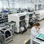
A fabricated printed circuit board (PCB) is the foundation of an electronic product. It contains copper traces, pads, drilled holes, solder mask, and silkscreen, but a bare PCB cannot perform its intended function until electronic components are installed and electrically connected.
The PCB assembly process, commonly referred to as PCBA, transforms a bare PCB into a fully functional electronic assembly. The process involves mounting components, soldering them to the board, inspecting solder joints, performing electrical and functional tests, and preparing the finished assembly for delivery.
Unlike PCB fabrication, which focuses on producing the physical circuit board, PCB assembly focuses on populating that board with electronic components and verifying that the completed assembly works according to the design requirements.
Depending on the product, component mix, board complexity, and production volume, a typical PCB assembly process may include DFM/DFA review, solder paste printing, SMT component placement, reflow soldering, SPI, AOI, X-ray inspection, THT assembly, wave or selective soldering, cleaning, electrical testing, functional testing, conformal coating, packaging, and shipment.
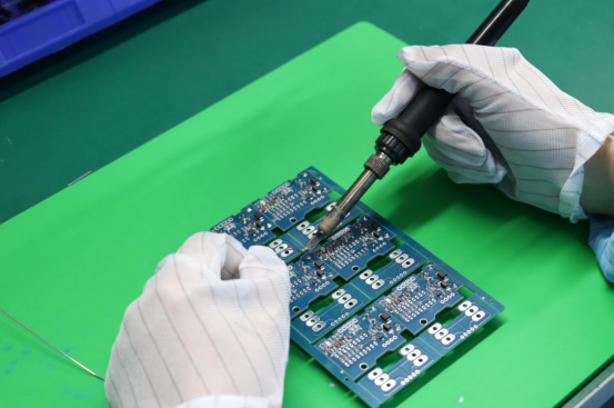
As an experienced PCB manufacturer and PCB assembly service provider, Kingda provides integrated solutions covering PCB prototype manufacturing, quick-turn PCB prototypes, PCB fabrication, SMT assembly, THT assembly, inspection and testing, NPI, small-batch production, and volume manufacturing. This allows customers to move efficiently from initial design verification to reliable production.
PCB Assembly Process at a Glance
The exact PCB assembly process varies according to the product and manufacturing requirements, but most assemblies follow a similar workflow:
- Design Review and Manufacturing Data Preparation
PCB fabrication and assembly files, BOM, pick-and-place data, and assembly drawings are reviewed for DFM and DFA requirements. - Solder Paste Printing
A precision stencil deposits controlled amounts of solder paste onto the PCB pads. - SMT Component Placement
Automated pick-and-place equipment accurately positions surface-mount components onto the solder paste deposits. - Reflow Soldering
The populated PCB passes through a controlled reflow oven, melting the solder paste and forming reliable electrical and mechanical connections. - Inspection
SPI, AOI, and X-ray inspection are used to verify solder paste quality, component placement, solder joints, and hidden connections. - Through-Hole Assembly
Through-hole components are installed and soldered using wave soldering, selective soldering, or manual soldering, depending on the application. - Cleaning
Flux residues and other contaminants are removed when required by the product or process specification. - Electrical and Functional Testing
ICT, Flying Probe Testing, and functional testing verify electrical performance and product functionality. - Final Inspection, Coating, Packaging, and Shipment
When required, conformal coating, EMI shielding, labeling, traceability, ESD protection, and specialized packaging are completed before shipment.
This structured approach enables Kingda to support projects ranging from PCB prototypes and engineering samples to low-volume and high-volume PCB assembly.
Before PCB Assembly: Design Review and Manufacturing Data Preparation
Before production begins, the assembly engineering team reviews the complete manufacturing package. This stage is essential because many PCB assembly problems can be prevented before the first board enters the SMT line.
A typical assembly package includes:
- Gerber or ODB++ files
- Bill of Materials (BOM)
- Pick-and-place / centroid files
- Assembly drawings
- NC drill files
- PCB fabrication drawings
- Solder paste stencil data
- Component specifications and approved manufacturer part numbers
- Special assembly and testing requirements
Engineers review component footprints, pad dimensions, component spacing, polarity markings, board-edge clearance, thermal requirements, fiducial locations, and other manufacturing details.
The objective is to identify potential problems such as:
- Incorrect footprints
- Insufficient component clearance
- Difficult-to-access solder joints
- Incorrect polarity information
- Missing components
- Conflicting BOM information
- Inadequate test points
- DFM or DFA issues
A professional DFM review can significantly reduce manufacturing risks because correcting a design issue before production is generally much easier and less costly than correcting defective assemblies after production begins.
Kingda Advantage
Kingda combines PCB manufacturing and PCB assembly capabilities, allowing engineers to evaluate the relationship between PCB fabrication and assembly requirements at an early stage.
For prototype and NPI projects, Kingda can support customers with design review, DFM analysis, PCB prototype manufacturing, component sourcing, assembly process planning, inspection, and testing, helping shorten the transition from design verification to production.
Surface Mount Technology (SMT) Assembly
Surface Mount Technology (SMT) is the primary assembly method used for many modern electronic products.
Unlike through-hole components, SMT components are mounted directly onto pads on the surface of the PCB. SMT enables smaller components, higher component density, double-sided assembly, and highly automated manufacturing.
A typical SMT process includes solder paste printing, SPI, component placement, and reflow soldering.
Step 1: Solder Paste Printing
The PCB assembly process begins with the application of solder paste to the PCB pads.
A stainless-steel SMT stencil is manufactured with precisely designed apertures corresponding to the solder pads. The stencil is aligned with the PCB, and a squeegee forces solder paste through the openings.
The solder paste generally contains powdered solder alloy and flux. For lead-free applications, alloys such as SAC305 are commonly used.
The quality of solder paste printing directly affects the subsequent soldering process.
If too little solder paste is deposited, the resulting joint may be weak or electrically open. Excessive solder paste can result in solder bridging, particularly on fine-pitch components.
Important parameters include:
- Paste volume
- Paste height
- Paste area
- Stencil alignment
- Aperture dimensions
- Printing pressure
- Squeegee speed
- Stencil thickness
Step 2: Solder Paste Inspection (SPI)
After printing, Solder Paste Inspection (SPI) verifies the quality of the solder paste deposits before components are placed.
Modern 3D SPI systems can measure:
- Solder paste volume
- Paste height
- Paste area
- X/Y offset
- Printing consistency
- Missing paste
- Excessive paste
- Bridging
SPI provides an important early quality checkpoint.
Instead of waiting until after reflow to discover solder-related defects, manufacturers can identify printing problems immediately and adjust the process.
This approach helps improve first-pass yield (FPY) and reduce unnecessary rework.
Step 3: SMT Component Placement
After SPI, the PCB moves to an automated pick-and-place machine.
Components are supplied through reels, trays, tubes, or other feeders. The machine uses precision nozzles to pick components and place them onto the corresponding solder paste deposits.
Vision systems verify component position, orientation, and polarity.
Modern placement systems can handle a wide range of components, including:
- 0201 and smaller passive components
- QFP
- QFN
- BGA
- LGA
- SOIC
- Connectors
- ICs
- Power components
- Large passive components
Accurate component placement is particularly important for fine-pitch components and high-density PCB assemblies.
Poor placement can result in:
- Tombstoning
- Misalignment
- Solder bridging
- Open solder joints
- Polarity errors
- Insufficient solder contact
For complex products, placement accuracy, feeder management, component verification, and machine calibration are critical to maintaining consistent assembly quality.
Step 4: Reflow Soldering
Once SMT components have been placed, the PCB passes through a controlled reflow soldering process.
The reflow oven uses multiple temperature zones to gradually heat the PCB, activate the flux, melt the solder alloy, and then cool the assembly under controlled conditions.
A typical lead-free reflow profile may include:
| Reflow Stage | Typical Function |
|---|---|
| Preheat | Gradually increases PCB and component temperature |
| Soak | Stabilizes thermal distribution and activates flux |
| Reflow | Melts solder and forms solder joints |
| Cooling | Solidifies solder and controls thermal stress |
The exact temperature profile depends on:
- Solder alloy
- PCB thickness
- Number of copper layers
- Component density
- Component thermal mass
- PCB material
- Moisture sensitivity
- Manufacturer recommendations
An optimized reflow profile helps prevent defects such as cold solder joints, solder balls, component damage, excessive voiding, and thermal stress.
For high-reliability products, thermal profiling should be validated during NPI and whenever significant process or material changes occur.
Step 5: Automated Optical Inspection (AOI)
After reflow soldering, the assembled PCB undergoes Automated Optical Inspection (AOI).
AOI systems use cameras, lighting, image processing, and inspection algorithms to identify visible defects.
Typical AOI inspection items include:
Component Defects
- Missing components
- Incorrect components
- Misaligned components
- Rotated components
- Polarity errors
- Lifted leads
Solder Defects
- Solder bridges
- Insufficient solder
- Excessive solder
- Solder balls
- Open solder joints
- Tombstoning
AOI is particularly valuable for high-volume production because it provides rapid and repeatable inspection.
However, optical inspection cannot reliably see solder joints hidden underneath components such as BGAs and some QFNs/LGAs. These applications may require X-ray inspection.
Step 6: X-Ray Inspection
X-ray inspection, also known as Automated X-Ray Inspection (AXI), provides visibility into solder joints that cannot be inspected optically.
X-ray inspection is particularly useful for:
- BGA packages
- QFN packages
- LGA packages
- Bottom-terminated components
- Hidden solder joints
- Through-hole solder fill
- Internal structural analysis
Depending on the application, manufacturers may use 2D X-ray or more advanced 3D CT/X-ray inspection.
X-ray inspection can help identify:
- Solder voids
- Insufficient solder
- Bridging
- Missing solder connections
- Misalignment
- Poor solder fill
For high-reliability PCB assemblies, X-ray inspection provides an additional layer of quality assurance that complements AOI and electrical testing.
Step 7: Through-Hole Technology (THT) Assembly
Not every component is suitable for SMT.
Large connectors, transformers, power components, switches, and mechanically stressed components may require Through-Hole Technology (THT).
THT components have leads that pass through drilled holes in the PCB and are soldered to pads.
Common THT soldering methods include:
Wave Soldering
Wave soldering passes the PCB over a controlled wave of molten solder. It is suitable for assemblies containing a significant number of through-hole components.
Selective Soldering
Selective soldering uses a programmable solder nozzle to solder individual through-hole joints without exposing the entire PCB to a solder wave.
It is especially useful for mixed-technology PCB assemblies where SMT components have already been soldered.
Hand Soldering
Manual soldering may be used for:
- Prototypes
- Engineering samples
- Low-volume production
- Large components
- Components with unusual locations
- Repair and rework
The appropriate method depends on board design, component quantity, thermal requirements, production volume, and quality requirements.
Step 8: PCB Cleaning
After soldering, some PCB assemblies require cleaning to remove flux residues and other contaminants.
Depending on the soldering materials and product requirements, manufacturers may use:
- Deionized water cleaning
- Aqueous cleaning
- Specialized cleaning agents
- Controlled spray cleaning
- Manual cleaning for selected areas
However, not every assembly requires washing.
When a qualified no-clean solder paste process is used and the residue meets the product requirements, post-solder cleaning may not be necessary.
For products used in demanding environments, cleanliness can be particularly important because contamination may affect insulation resistance, conformal coating adhesion, corrosion resistance, or long-term reliability.
Step 9: Electrical Testing and Functional Testing
Visual inspection alone cannot confirm that an electronic assembly actually functions correctly.
Therefore, many PCB assembly projects require electrical and functional testing.
In-Circuit Testing (ICT)
ICT uses a test fixture with multiple probes to access designated test points on the PCB.
It can verify parameters such as:
- Component values
- Shorts
- Opens
- Continuity
- Resistance
- Capacitance
- Certain circuit characteristics
ICT is particularly suitable for medium- and high-volume production where fixture costs can be distributed across a larger quantity of boards.
Flying Probe Testing
Flying Probe Testing (FPT) uses movable probes to contact test points without requiring a dedicated bed-of-nails fixture.
It is well suited for:
- PCB prototypes
- Engineering samples
- Low-volume PCB assembly
- Frequently revised designs
- Complex boards
Flying probe testing offers greater flexibility, while ICT can provide faster testing for suitable high-volume applications.
Functional Testing
Functional testing powers the completed PCB and verifies whether the assembly performs its intended functions.
Depending on the product, functional testing may verify:
- Voltage outputs
- Current consumption
- Communication interfaces
- Sensors
- Displays
- Motors
- Relays
- Wireless communication
- Control functions
For products requiring high reliability, additional tests such as burn-in or environmental testing may also be specified.
Step 10: Final Inspection, Coating, Packaging, and Shipment
After assembly and testing, the finished PCB assembly undergoes final inspection.
The inspection may include:
- Component verification
- Solder joint review
- Connector inspection
- PCB cleanliness
- Mechanical inspection
- Label verification
- Serial number verification
- Traceability confirmation
- Functional test status
Conformal Coating
For applications exposed to moisture, dust, chemicals, condensation, or harsh environments, conformal coating may be applied.
Common coating materials include:
- Acrylic
- Silicone
- Polyurethane
- Epoxy
- Parylene
The coating protects the assembled PCB against environmental contamination and can improve long-term reliability when correctly specified and applied.
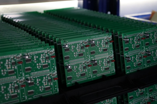
EMI Shielding
Some electronic products require EMI shielding to control electromagnetic interference.
Shielding can help protect sensitive circuits from external interference while also reducing emissions generated by the PCB assembly.
Packaging
Finished PCB assemblies should be packaged according to their sensitivity and shipping conditions.
Typical packaging may include:
- ESD-safe bags
- Moisture barrier bags
- Desiccants
- Humidity indicator cards
- Anti-static trays
- Protective foam
- Reinforced cartons
Proper packaging helps protect components from electrostatic discharge, moisture, mechanical shock, and contamination during storage and transportation.
Turnkey, Partial-Turnkey, and Consigned PCB Assembly
Customers can choose different PCB assembly service models depending on their supply-chain strategy.
Full Turnkey PCB Assembly
The assembly provider manages:
- PCB fabrication
- Component sourcing
- PCB assembly
- Inspection
- Testing
- Packaging
This model provides a simplified supply chain and reduces the customer’s purchasing workload.
Partial-Turnkey Assembly
The customer supplies selected components or materials while the assembly manufacturer sources the remaining parts.
This approach is useful when customers have preferred suppliers or proprietary components.
Consigned PCB Assembly
The customer provides the PCB and components, while the assembly provider handles:
- SMT placement
- THT assembly
- Soldering
- Inspection
- Testing
- Packaging
This model provides greater customer control over component sourcing.
Kingda PCB Assembly Capabilities
As an experienced PCB manufacturer and PCB assembly service provider, Kingda supports customers throughout the entire electronics manufacturing lifecycle.
Our capabilities cover:
PCB Design Review → DFM Engineering Review → PCB Prototype Manufacturing → PCB Assembly → Inspection & Testing → Design Optimization → Small-Batch Production → Volume Manufacturing
Kingda’s integrated capabilities provide several advantages.
1. PCB Manufacturing and PCB Assembly Integration
By combining PCB fabrication and PCBA services, Kingda can coordinate board manufacturing and assembly requirements more efficiently.
This reduces communication gaps between separate suppliers and helps identify fabrication or assembly risks earlier.
2. Prototype to Volume Production
Kingda supports projects from PCB prototypes and quick-turn PCB assembly to low-volume production and high-volume manufacturing.
This allows customers to continue working with the same manufacturing partner as their products move through different development stages.
3. SMT and THT Assembly
Kingda provides both SMT assembly and THT assembly, supporting mixed-technology boards and a wide range of component packages.
4. Component Sourcing Support
A reliable BOM and component supply chain is essential for PCBA production.
Kingda can support component sourcing and BOM management while helping customers address availability, lifecycle, and substitution considerations.
5. Comprehensive Inspection and Testing
Quality control can include:
- SPI
- AOI
- X-ray inspection
- Visual inspection
- Flying probe testing
- ICT
- Functional testing
- Rework and repair
The inspection strategy can be adapted to product complexity, production volume, and reliability requirements.
6. NPI and DFM Support
For new products, Kingda can support New Product Introduction (NPI) with engineering review, manufacturing feedback, prototype assembly, testing, and design optimization.
This helps customers identify manufacturing issues before entering mass production.
7. Quality and Traceability
A controlled manufacturing process, documented inspection procedures, component traceability, and production records help provide consistent quality across prototype and production builds.
For demanding applications, manufacturing and inspection requirements can be aligned with applicable industry standards and customer specifications.
How to Improve PCB Assembly Manufacturability
Engineers can significantly improve the PCB assembly process by considering manufacturing requirements during the design stage.
Important considerations include:
- Use appropriate component footprints
- Maintain adequate component spacing
- Provide sufficient solder mask clearance
- Use proper fiducial marks
- Consider component orientation
- Avoid unnecessary component density
- Provide accessible test points
- Design appropriate thermal relief
- Follow recommended BGA escape and via structures
- Consider panelization requirements
- Maintain accurate BOM information
- Define polarity markings clearly
- Design for both SMT and THT process requirements
A strong DFM/DFA strategy reduces manufacturing uncertainty and can improve yield, reliability, cost, and production efficiency.
PCB Assembly Process for Different Production Volumes
The manufacturing strategy may change depending on production volume.
| Production Stage | Typical Manufacturing Focus |
|---|---|
| PCB Prototype | Fast turnaround, design verification, flexible sourcing |
| NPI | DFM/DFA validation, process optimization, first-article inspection |
| Low-Volume PCB Assembly | Flexible production, flying probe testing, efficient setup |
| Medium-Volume Production | Process standardization, automated inspection, controlled sourcing |
| High-Volume PCB Assembly | Automation, optimized cycle time, SPC, yield improvement, traceability |
The most suitable production process should therefore be selected according to the product lifecycle rather than simply the number of boards being ordered.
PCB Assembly Process Summary
The PCB assembly process is a controlled sequence that transforms a fabricated PCB into a fully functional electronic assembly.
From DFM review and solder paste printing to SMT component placement, reflow soldering, AOI, X-ray inspection, THT assembly, electrical testing, functional testing, and final packaging, every stage contributes to the quality and reliability of the finished product.
For engineers, understanding the complete PCBA manufacturing process helps improve design manufacturability and reduce production problems. For procurement teams, understanding assembly capabilities makes it easier to select an appropriate manufacturing partner. For product developers, an integrated manufacturing solution can simplify the transition from PCB prototype to small-batch and volume production.
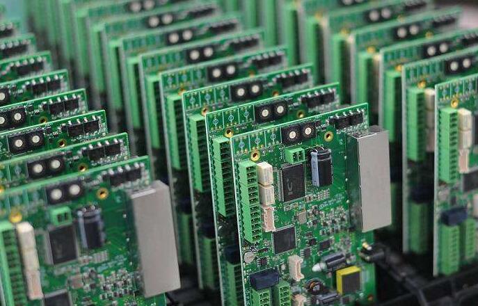
With experience in PCB manufacturing and PCB assembly, Kingda provides integrated manufacturing support covering PCB prototypes, quick-turn PCB fabrication, SMT assembly, THT assembly, inspection, testing, NPI, small-batch production, and volume manufacturing.
Whether you are developing your first prototype or preparing an established product for mass production, Kingda can provide a coordinated PCB and PCBA manufacturing solution tailored to your technical and production requirements.
From PCB prototype to reliable PCBA production, Kingda supports your product at every stage.