What Are RF and Microwave PCBs?
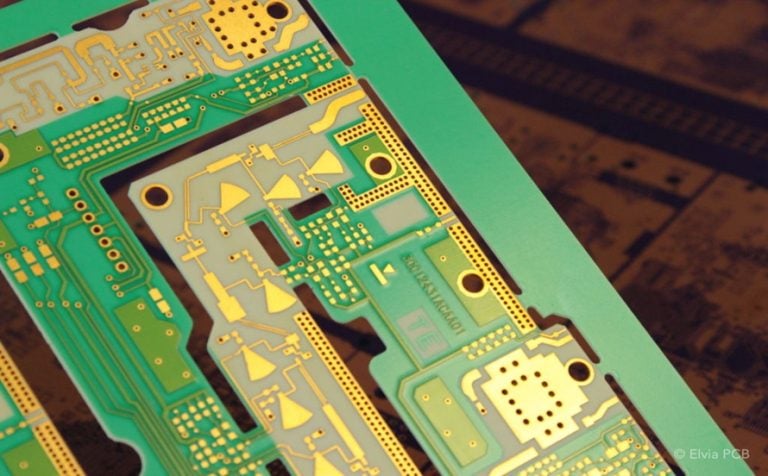
An RF PCB is a printed circuit board designed to transmit, receive, distribute, or process radio-frequency signals. RF refers broadly to electromagnetic signals used for wireless communication and other applications. Depending on the industry and application, RF circuits can operate from relatively low frequencies into the microwave range.
A Microwave PCB is designed for higher-frequency applications where transmission-line effects, dielectric properties, conductor losses, impedance control, and electromagnetic coupling become increasingly important.
There is no single universal frequency boundary that separates RF from microwave technology. In engineering practice, the terms often overlap. Microwave applications are commonly associated with frequencies above approximately 1 GHz, while millimeter-wave applications can extend into tens or hundreds of gigahertz.
Modern wireless technologies make extensive use of RF and microwave circuits. Examples include cellular communication, 5G infrastructure, Wi-Fi, GNSS, radar, satellite communication, automotive sensing, and specialized medical equipment.
As operating frequency increases, PCB traces can no longer be treated simply as ideal electrical connections. Their physical dimensions, dielectric environment, copper surface roughness, layer structure, connectors, vias, and return-current paths can all influence electrical performance.
For this reason, RF and Microwave PCB design requires a closer integration of electrical design, material selection, manufacturing engineering, and testing than many conventional PCB applications.
Key Advantages of RF and Microwave PCBs
RF and microwave circuit boards provide several important advantages for high-frequency electronic systems.
Low Signal Loss
Signal attenuation becomes an increasingly important consideration as frequency increases.
A properly designed High-Frequency PCB can reduce conductor loss, dielectric loss, reflection loss, and other transmission losses.
Low-loss materials, controlled impedance, appropriate copper surfaces, optimized stackups, and carefully designed transmission lines can help preserve signal quality over the required transmission distance.
Reducing unnecessary signal loss can also improve system efficiency and reduce the amount of transmit power required to achieve the desired performance.
High-Speed Data Transmission
High-frequency PCB technology supports high-speed signal transmission required by modern communication systems.
Applications such as 5G, Wi-Fi, satellite communications, high-speed networking, radar, and advanced wireless systems rely on carefully controlled RF and microwave signal paths.
As data rates and operating frequencies increase, designers must pay greater attention to insertion loss, return loss, crosstalk, impedance discontinuities, and signal reflections.
Excellent Signal Integrity
Signal Integrity is one of the most important considerations in RF and microwave PCB design.
At high frequencies, even small changes in trace geometry, dielectric thickness, connector structure, via configuration, or reference-plane continuity can affect signal behavior.
A well-designed RF PCB helps control:
- Impedance
- Insertion loss
- Return loss
- Crosstalk
- Reflection
- Electromagnetic coupling
- Phase consistency
- Transmission-line performance
Maintaining signal integrity is particularly important in systems where weak received signals must be accurately detected and processed.
Efficient Thermal Management
RF and microwave systems can contain power amplifiers, transceivers, processors, and other heat-generating components.
Although thermal performance is not determined simply by using a high-frequency laminate, appropriate materials and PCB structures can contribute to effective thermal management.
Designers may use copper planes, thermal vias, copper-filled structures, heat spreaders, metal-backed structures, or external thermal solutions depending on the power level and application.
Good thermal management helps maintain stable electrical characteristics and improves long-term component reliability.
Compact High-Frequency System Design
RF and microwave technology allows manufacturers to integrate wireless functions into compact electronic products.
By optimizing the PCB stackup, transmission lines, antenna structures, shielding, and component placement, engineers can achieve high-frequency functionality within limited physical space.
This is particularly valuable in mobile communications, automotive electronics, aerospace systems, and portable wireless devices.
Applications of RF and Microwave PCBs
RF and Microwave PCB technology is used wherever electronic systems need to generate, transmit, receive, or process high-frequency signals.
Radar Systems
Radar systems use radio-frequency and microwave signals to detect objects and determine parameters such as distance, direction, and velocity.
Military radar, aviation systems, marine radar, weather radar, industrial sensing, and automotive radar all require carefully designed RF signal paths.
Automotive radar commonly operates in frequency bands such as 24 GHz and 77–81 GHz, where PCB material selection, antenna integration, impedance control, and manufacturing tolerances become especially important.
At these frequencies, even relatively small manufacturing variations can affect electrical performance.
GNSS and Navigation
Global Navigation Satellite System (GNSS) technologies, including GPS, Galileo, BeiDou, and GLONASS, use RF signals transmitted from satellites.
GNSS receiver PCBs must provide low-loss signal paths and accurate impedance control because the received satellite signals can be relatively weak.
Antenna routing, RF filtering, grounding, shielding, and low-noise amplifier layout are therefore important aspects of GNSS PCB design.
Telecommunications
Telecommunications is one of the largest application areas for RF PCB technology.
5G infrastructure, cellular communication systems, Wi-Fi equipment, Bluetooth devices, base stations, RF modules, and other wireless communication products require carefully controlled high-frequency signal paths.
Modern wireless systems may operate across multiple frequency bands, making material selection, impedance control, antenna design, and electromagnetic compatibility increasingly important.
Industrial Automation
Wireless industrial equipment can use RF and microwave circuits for communication, sensing, monitoring, and control.
Industrial environments can contain significant electrical noise, electromagnetic interference, vibration, temperature variation, and other challenging conditions.
An appropriately designed RF PCB Design can help maintain reliable wireless communication and signal performance under these conditions.
Medical Equipment
RF and microwave circuits are used in various medical and diagnostic systems.
Applications can include imaging equipment, RF generators, wireless medical devices, monitoring systems, and specialized therapeutic equipment.
Medical RF systems often require strict control of noise, electromagnetic compatibility, thermal behavior, and signal accuracy.
Broadcasting
Broadcasting systems use RF circuits to transmit and receive radio, television, and other wireless signals.
Although some broadcast systems operate at relatively lower frequencies than modern microwave systems, the PCB still needs to maintain appropriate impedance, signal routing, grounding, and electromagnetic compatibility.
Challenges in RF and Microwave PCB Design and Manufacturing
High-frequency signals are more sensitive to PCB geometry and material properties than many conventional digital signals.
As frequency increases, PCB traces behave increasingly like transmission lines rather than simple electrical wires. This creates additional challenges during both design and manufacturing.
Impedance Control
Maintaining controlled impedance is one of the most important requirements in RF PCB Design.
Transmission-line impedance depends on factors such as:
- Trace width
- Copper thickness
- Dielectric thickness
- Dielectric constant
- Trace geometry
- Reference-plane structure
- Copper surface characteristics
Common RF systems may use 50 Ω single-ended transmission lines, while differential high-speed systems may use other impedance values depending on the application.
An impedance-controlled design requires close coordination between the PCB designer and manufacturer.
Manufacturing tolerances in trace width, dielectric thickness, copper thickness, and layer registration can directly affect the final impedance.
High-Frequency Material Selection
Material selection is critical for a High-Frequency PCB.
Conventional FR-4 materials may be suitable for some lower-frequency RF applications, but specialized low-loss laminates may be preferred when operating frequency, loss budget, stability, or electrical performance becomes more demanding.
Important material characteristics include:
- Dielectric constant (Dk)
- Dissipation factor (Df)
- Thermal conductivity
- Coefficient of thermal expansion
- Moisture absorption
- Dimensional stability
- Copper adhesion
- Surface roughness
Depending on the application, designers may consider PTFE-based materials, hydrocarbon/ceramic laminates, or other low-loss high-frequency materials.
Material selection should be based on the actual frequency range and electrical requirements rather than assuming that one material is suitable for every RF application.
Signal Loss and Surface Roughness
Conductor loss becomes increasingly significant at higher frequencies.
The skin effect causes high-frequency current to concentrate near the conductor surface. As a result, copper surface roughness can influence conductor loss and transmission-line performance.
For demanding microwave designs, the manufacturer may need to control copper foil type, surface treatment, copper roughness, plating thickness, and etching quality.
Thermal Management
High-frequency systems may include power amplifiers and other components that generate substantial heat.
Thermal management must therefore be considered together with electrical performance.
Thermal vias, copper planes, heat spreaders, appropriate materials, and optimized component placement can help control temperature.
Designers should also consider how temperature changes affect dielectric properties, dimensions, impedance, and component performance.
Electromagnetic Compatibility
Electromagnetic compatibility (EMC) is particularly important for RF and microwave systems.
Poor PCB layout can cause unwanted radiation, coupling, interference, or susceptibility to external electromagnetic energy.
Effective EMC strategies may include:
- Continuous ground structures
- Appropriate shielding
- Controlled return paths
- Short RF connections
- Proper via stitching
- Filtering
- Careful component placement
- Controlled antenna structures
EMC should be considered during the initial PCB design rather than treated only as a final-stage testing requirement.
Tight Manufacturing Tolerances
As operating frequency increases, manufacturing tolerances can have a greater effect on electrical performance.
Small variations in dielectric thickness, trace width, copper thickness, layer registration, and via geometry can change impedance and signal loss.
For this reason, manufacturers producing microwave boards need appropriate process control and measurement capabilities.
Surface Finish Selection
Surface finish can also affect high-frequency performance, particularly in RF structures where conductor loss and surface characteristics are important.
The finish should be selected according to the electrical design, component requirements, soldering process, reliability requirements, and manufacturing process.
The designer and manufacturer should evaluate whether the selected surface treatment is appropriate for the exposed RF conductors and high-frequency transmission paths.
Cost Control
Microwave PCB Manufacturing generally costs more than standard PCB fabrication.
Cost can be affected by:
- High-frequency laminate selection
- Number of layers
- Board dimensions
- Copper thickness
- Controlled-impedance requirements
- Manufacturing tolerances
- Surface finish
- Via technology
- Testing requirements
- Material availability
Using unnecessarily expensive materials does not always improve the final product. The material and manufacturing process should instead be selected according to the actual electrical and reliability requirements.
RF PCB vs. Microwave PCB
RF and microwave PCBs are closely related technologies, and their frequency ranges can overlap.
| Feature | RF PCB | Microwave PCB |
|---|---|---|
| Typical frequency | Broad range, from MHz into GHz | Commonly associated with higher GHz frequencies |
| Main concern | RF transmission and reception | High-frequency transmission and microwave behavior |
| Material requirements | FR-4 or specialized RF materials depending on frequency | Often requires low-loss specialized materials |
| Impedance control | Important | Extremely important |
| Manufacturing tolerance | Application-dependent | Often more demanding |
| Typical applications | Radio, wireless communication, GNSS, RF modules | Radar, satellite, 5G infrastructure, microwave communication |
| Cost | Moderate to high | Generally higher |
It is important to understand that the boundary between RF and microwave is not absolute. The appropriate PCB technology depends on the operating frequency, bandwidth, signal power, loss budget, environmental conditions, and system architecture.
RF and Microwave PCB Design Guidelines
A successful RF PCB Design requires electrical performance and manufacturing capability to be considered together.
Keep RF Signal Paths Short
RF traces should generally be kept as short and direct as practical.
Unnecessary bends, transitions, connectors, and vias can introduce additional discontinuities and losses.
Maintain a Continuous Reference Plane
High-frequency signals require a predictable return-current path.
A continuous ground or reference plane beneath the transmission line can help control impedance and reduce unwanted electromagnetic coupling.
Optimize Trace Geometry
Trace width should be calculated according to the required impedance, dielectric thickness, material properties, and copper thickness.
Rather than relying on a generic trace-width rule, designers should use the actual stackup parameters provided by the manufacturer.
Minimize Unnecessary Via Transitions
Every via transition can introduce parasitic inductance, capacitance, and impedance discontinuity.
Where practical, RF transmission paths should minimize unnecessary layer changes.
When vias are unavoidable, their geometry and surrounding reference structure should be carefully designed.
Use Ground Via Stitching
Ground via stitching can help provide a low-inductance return path and improve electromagnetic isolation between circuit sections.
The appropriate via spacing depends on the operating frequency and PCB structure and should be determined according to the specific design.
Separate Sensitive RF Circuits
Sensitive RF receiver circuits should be appropriately separated from noisy digital or power sections.
Component placement, grounding, shielding, filtering, and routing should work together to reduce unwanted coupling.
Consider the Antenna During PCB Design
In many wireless products, the antenna and RF transmission line cannot be treated as completely independent structures.
The antenna geometry, PCB dielectric environment, ground plane, enclosure, nearby components, and transmission-line impedance can all influence antenna performance.
Therefore, antenna design should be considered from the beginning of the PCB development process.
RF and Microwave PCB Manufacturing Process
The manufacturing process for a Microwave PCB is similar to conventional PCB fabrication in many basic respects, but tighter control may be required for material handling, dimensional tolerances, impedance, copper geometry, and surface characteristics.
A typical process includes:
Engineering Review → Material Preparation → Inner-Layer Fabrication → Lamination → Drilling → Copper Plating → Outer-Layer Fabrication → Solder Mask → Surface Finish → Electrical Testing → Final Inspection
For high-frequency applications, additional engineering controls may include:
- Controlled dielectric thickness
- Impedance coupon fabrication
- Copper roughness control
- Precise layer registration
- Controlled etching
- Material-specific lamination profiles
- High-frequency electrical testing
- RF performance verification
The actual process should be customized according to the laminate system and electrical requirements.
How to Choose an RF and Microwave PCB Manufacturer
Choosing the right manufacturer is an important part of RF and microwave product development.
Unlike ordinary PCB production, high-frequency boards require close coordination between design engineering and manufacturing engineering.
Before selecting a supplier, customers should evaluate:
High-Frequency Material Experience
The manufacturer should understand the processing characteristics of the selected high-frequency laminate.
Different materials may require different drilling, lamination, routing, plating, and handling processes.
Controlled-Impedance Capability
The manufacturer should be able to control and verify the required impedance.
This includes maintaining appropriate control over trace geometry, dielectric thickness, copper thickness, and layer registration.
Manufacturing Tolerance Control
High-frequency applications may require tighter tolerances than conventional PCB products.
The supplier should have appropriate process-control procedures and inspection equipment.
Engineering Support
A capable engineering team can identify potential problems before production.
Early DFM and manufacturability reviews can help prevent issues related to stackup, impedance, material selection, drilling, routing, and assembly.
Testing Capability
Testing requirements vary significantly between RF applications.
Depending on the project, testing may include electrical continuity testing, impedance testing, dimensional inspection, thermal evaluation, RF performance testing, and other specialized measurements.
Why Choose Kingda for RF and Microwave PCB Manufacturing?
RF and microwave boards require a combination of specialized materials, precise PCB design, controlled manufacturing processes, and professional engineering support.
Kingda can provide customized RF and Microwave PCB solutions based on different frequency ranges, layer structures, materials, impedance requirements, and application environments.
Our engineering team can work with customers during the design and manufacturing stages to evaluate key factors such as:
- High-frequency material selection
- PCB stackup
- Controlled impedance
- Signal routing
- Copper thickness
- Dielectric thickness
- Via structures
- Thermal management
- Surface finish
- Manufacturing tolerances
- Electrical testing
Customized Manufacturing Solutions
Different RF applications have different requirements.
Kingda can help customers select suitable materials, stackup configurations, copper structures, and manufacturing processes according to the actual product specifications.
Professional Engineering Support
Engineering communication is particularly important for high-frequency PCBs.
Potential manufacturability issues can be identified during the engineering review before production begins, helping reduce unnecessary design iterations.
Quality-Focused Production
High-frequency PCB performance depends heavily on dimensional and material consistency.
Kingda focuses on process control throughout PCB fabrication to help maintain stable electrical and mechanical performance.
Support from Prototype to Production
RF and microwave products often require several engineering iterations before reaching mass production.
Kingda can support customers through prototype fabrication, PCB Assembly, testing, design optimization, and production preparation.
This helps create a smoother transition from the initial RF prototype to stable volume production.
Conclusion
RF PCB and Microwave PCB technologies are essential for modern wireless communication, radar, navigation, telecommunications, automotive sensing, medical equipment, and other high-frequency applications.
As frequency increases, PCB traces behave increasingly like transmission lines, making impedance, dielectric properties, conductor loss, surface roughness, electromagnetic compatibility, and manufacturing tolerances critical design considerations.
A successful High-Frequency PCB therefore requires more than simply selecting a specialized laminate. Designers must consider the complete electrical and mechanical structure, while manufacturers must maintain tight control over materials, dimensions, layer registration, copper geometry, and testing.
By combining appropriate RF PCB Design, suitable materials, controlled Microwave PCB Manufacturing, and professional engineering support, manufacturers can achieve reliable high-frequency performance while maintaining an appropriate balance between quality, cost, and production efficiency.
For RF and microwave PCB projects, Kingda can provide customized manufacturing support from prototype development through production, helping customers turn demanding high-frequency PCB designs into reliable finished products.