What Is a Semi-Flex PCB?
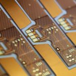
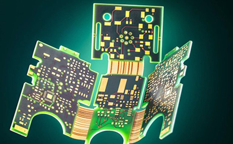
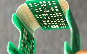
A Semi-Flex PCB, also known as a Semi-Flexible PCB or FR4 semi-flexible circuit board, is a specialized PCB structure that introduces localized flexibility into an otherwise rigid circuit board.
Unlike a conventional rigid-flex PCB, which combines rigid materials such as FR-4 with a dedicated flexible substrate such as polyimide, a semi-flexible PCB is generally manufactured from a rigid material system, most commonly FR-4. Flexibility is created by selectively reducing the thickness of specific areas of the PCB, usually through controlled milling or depth routing.
After the selected region has been thinned, the remaining material becomes sufficiently thin to allow controlled bending or folding without immediately damaging the board. The rest of the PCB retains its normal rigid structure and provides a stable platform for component mounting.
This construction makes an FR4 Semi-Flex PCB particularly suitable for applications requiring limited or one-time bending during assembly or installation. It should not normally be treated as a replacement for a dynamic flexible circuit that must repeatedly bend during operation.
In a typical semi-flex design, electronic components are placed on the rigid sections rather than the thinned flexible areas. This helps protect components and solder joints from mechanical stress and preserves the intended flexibility of the bend zone.
In simple terms, a semi-flex PCB can be viewed as a rigid FR-4 board with specially engineered thin sections that allow localized bending.
Semi-Flex PCB vs. Rigid-Flex PCB
Semi-flex and rigid-flex PCBs are sometimes confused because both technologies combine rigid and flexible regions. However, their material structures, mechanical performance, and intended applications are different.
Semi-Flex PCB
A Semi-Flexible PCB normally starts with a rigid material such as FR-4. Selected regions are mechanically thinned to create controlled bending areas.
Key characteristics include:
- Rigid and flexible regions are generally based on the same primary board material.
- Flexibility is created by reducing material thickness.
- Suitable for limited or static bending.
- Generally simpler and more economical than a true rigid-flex construction.
- Flexible sections are normally kept relatively short.
- Components should generally remain on rigid sections.
Rigid-Flex PCB
A rigid-flex PCB combines rigid PCB sections with dedicated flexible circuit layers, typically using polyimide-based flexible materials.
Compared with a Semi-Flex PCB, rigid-flex technology offers greater mechanical flexibility and is more suitable for applications involving repeated bending, longer flex sections, or more complex three-dimensional routing.
| Feature | Semi-Flex PCB | Rigid-Flex PCB |
|---|---|---|
| Primary construction | Rigid material with locally thinned areas | Rigid and dedicated flexible materials |
| Typical flexible material | FR-4 or similar rigid material system | Polyimide-based flexible circuit materials |
| Flexibility | Limited | Higher |
| Dynamic bending | Generally unsuitable | Suitable when properly designed |
| Manufacturing complexity | Relatively low | Higher |
| Cost | Generally lower | Generally higher |
| Typical application | Static installation bending | Repeated bending and 3D interconnection |
Therefore, the choice should be based on the actual mechanical requirements rather than simply the desired PCB price.
Advantages of Semi-Flex PCB
The Semi-Flex PCB structure provides several advantages for products that require limited mechanical flexibility without the cost or complexity of a dedicated rigid-flex design.
Controlled Flexibility
The primary advantage is the ability to introduce bending into selected sections of a rigid PCB.
A carefully designed thinned region can allow the board to fold into a predetermined position during assembly. This can help manufacturers package electronics into smaller housings while maintaining rigid areas for component mounting.
However, the bending capability is limited and should be defined according to the material thickness, remaining thickness, bend radius, copper structure, and manufacturing process.
Simplified Assembly
A semi-flex circuit can combine functions that might otherwise require several rigid PCBs connected by cables or connectors.
By integrating multiple rigid sections into one board and using localized flex areas as interconnects, the number of separate PCB assemblies and mechanical connections can potentially be reduced.
This can simplify assembly and reduce the amount of manual wiring required during final product integration.
Reduced Cable and Connector Requirements
For short-distance connections between circuit sections, a Semi-Flexible PCB can sometimes replace separate wires, cables, and connectors.
This can provide a cleaner internal structure and reduce the number of electrical interfaces. Fewer connectors may also reduce potential connection points that could be affected by vibration, contamination, or assembly variation.
Cost Efficiency
One of the main reasons manufacturers consider Semi-Flex PCB technology is cost.
Compared with a dedicated rigid-flex PCB, a semi-flex structure can often use a simpler material system and manufacturing process. It may also consolidate multiple rigid boards into a single PCB assembly.
Potential cost benefits can come from:
- Using a primarily rigid FR-4 material system.
- Reducing the number of separate PCB assemblies.
- Reducing cable and connector requirements.
- Simplifying mechanical assembly.
- Reducing the number of interconnection points.
The actual cost advantage depends on board size, layer count, material thickness, bending requirements, production volume, and manufacturing tolerances.
Improved Signal Integrity
Replacing external cables and connectors with PCB traces can provide more predictable electrical interconnections.
For high-speed applications, signal integrity depends on trace geometry, dielectric structure, reference planes, impedance control, connector transitions, and routing length. A properly designed semi-flex circuit can eliminate some connector and cable transitions and therefore simplify the overall signal path.
However, semi-flex should not automatically be considered a high-speed solution. The complete stackup and mechanical structure still need to be evaluated for controlled impedance and signal integrity.
Resistance to Vibration and Shock
A properly integrated PCB interconnect can eliminate some mechanically vulnerable cable connections.
This can be beneficial in applications exposed to vibration or mechanical movement. Nevertheless, the thinned flex region itself becomes a mechanically sensitive part of the PCB, so the design must account for bending stress, vibration, copper fatigue, and the location of components and vias.
Disadvantages of Semi-Flex PCB
Although Semi-Flex PCB technology offers important advantages, it also has limitations that must be considered before design and production.
Limited Bending Cycles
The most important limitation is that semi-flex circuits are generally intended for static or limited bending rather than continuous dynamic flexing.
Repeated bending can cause mechanical fatigue in the copper and surrounding dielectric structure. Over time, this may result in copper cracking, trace failure, delamination, or other reliability problems.
For applications where the circuit must repeatedly move during normal operation, a dedicated flexible PCB or rigid-flex PCB is usually more appropriate.
More Challenging Mechanical Design
Designing a semi-flex board requires careful consideration of the relationship between PCB thickness, remaining material thickness, bend radius, copper distribution, routing, and mechanical constraints.
A design that looks electrically correct may still fail mechanically if the flex region is too thin, too short, or subjected to excessive bending force.
Designers should therefore evaluate both electrical and mechanical requirements during the early design stage.
Limited Flexible Section Length
The flexible section of a semi-flex PCB is generally more restricted than that of a dedicated flexible circuit.
As the length of the thinned section increases, controlling mechanical stress becomes more difficult. Long flexible sections can also reduce structural stability and may not provide the reliability required for repeated movement.
When a design requires a long flexible tail or complex three-dimensional movement, rigid-flex or flexible PCB technology should be considered instead.
Component Placement Restrictions
Components, large pads, heavy copper structures, and mechanical features should generally be kept away from the flexible region.
Placing rigid or heavy components in the bend zone can increase mechanical stress and reduce the reliability of both the component solder joints and PCB traces.
Semi-Flex PCB Applications
The compact construction and localized bending capability of Semi-Flex PCB technology make it useful in a variety of applications.
Camera and Flash Modules
Compact camera systems often have limited internal space and require circuit sections to be folded into specific geometric configurations.
A semi-flex structure can allow several rigid PCB sections to be connected while folding the board into a compact form. This can reduce the need for separate cables and connectors and simplify the assembly of compact camera modules.
Medical Electronics
Portable medical equipment often requires a combination of compact packaging, mechanical reliability, and integrated electrical connections.
Semi-Flexible PCB technology can be used in selected handheld or compact medical devices where the flexible section only needs to be bent during assembly or installation.
For medical applications, material selection, cleanliness, reliability testing, and applicable regulatory requirements should be evaluated according to the final product.
Automotive Electronics
Automotive electronics frequently need to fit into irregular spaces while operating in environments involving vibration and temperature changes.
A Semi-Flex PCB can be useful for short-distance interconnections between rigid circuit sections when the board needs to be folded into a specific position during assembly.
Potential applications include instrument clusters, sensor modules, lighting systems, control modules, camera assemblies, and compact electronic interfaces.
However, automotive applications require careful evaluation of thermal cycling, vibration, humidity, copper fatigue, and long-term mechanical reliability.
Consumer Electronics
Compact consumer products often have strict space limitations.
Semi-flex technology can help circuit designers create folded PCB structures that fit inside small enclosures. Applications may include speakers, computer peripherals, cameras, displays, compact controllers, and other space-constrained electronic devices.
The technology can also help reduce cable assemblies and simplify internal product architecture.
Design Considerations for Semi-Flex PCB
Correct Semi-Flexible PCB Design is critical to achieving reliable performance. The following factors should be considered during PCB development.
Component and Via Placement
Components, through-holes, vias, and solder joints should generally be kept out of the thinned flex region unless the specific construction has been validated for them.
Heavy components should remain on rigid sections whenever possible. Their weight can create additional mechanical stress when the PCB is folded or subjected to vibration.
Component placement should also maintain sufficient clearance from the transition between the rigid and thinned regions.
Layer and Routing Management
The flexible section should generally use as few layers as practical.
Reducing the number of copper layers can improve flexibility and reduce mechanical stress. Copper should also be distributed carefully to avoid creating severe asymmetry in the bend region.
Routing should avoid sharp corners and unnecessary copper concentrations. Where appropriate, traces should follow the direction of bending and maintain sufficient spacing from mechanical transition zones.
Bend Radius
Bend radius is one of the most important parameters in Semi-Flexible PCB Design.
A smaller bend radius produces greater mechanical strain. If the bend is too sharp, the copper or dielectric material may crack or experience permanent damage.
The allowable bend radius depends on:
- Original PCB thickness.
- Remaining thickness in the milled region.
- Copper thickness.
- Number of copper layers.
- Material properties.
- Bend direction.
- Static or dynamic bending requirements.
The manufacturer’s recommended bend radius should be confirmed before production.
Static Bending Only
Most semi-flex designs are intended to be bent into position during assembly and then remain relatively stationary.
If the product requires repeated bending, twisting, or continuous movement during operation, a dedicated flexible PCB or rigid-flex PCB is generally a better choice.
Copper Distribution
Copper distribution has both electrical and mechanical effects.
The copper thickness must be sufficient to carry the required current without excessive temperature rise, while excessive copper in the bend region can increase stiffness.
For this reason, the designer must balance current-carrying capability, thermal performance, flexibility, and mechanical reliability.
Mechanical Stress Control
The thinned region should be designed to minimize concentrated mechanical stress.
Sudden transitions in thickness can create stress concentrations, so the transition geometry should be carefully controlled. The PCB should also be bent gradually rather than forced into a sharp angle during assembly.
Mechanical fixtures may be considered when repeatable bending is required during production.
Semi-Flex PCB Manufacturing Process
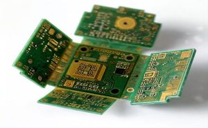
The manufacturing process for a Semi-Flex PCB is based on conventional rigid PCB fabrication combined with controlled mechanical thinning.
A typical process may include:
Material Preparation
FR-4 or another suitable rigid PCB material is selected according to the electrical, thermal, mechanical, and thickness requirements.
The laminate thickness is particularly important because it determines the amount of material that can be removed while maintaining sufficient structural strength.
PCB Fabrication
The basic PCB structure is manufactured using conventional processes such as imaging, copper patterning, lamination for multilayer boards, drilling, plating, solder mask application, surface finishing, and electrical testing.
The exact process depends on the board’s layer count and design requirements.
Controlled Milling or Depth Routing
After the basic PCB structure has been fabricated, selected regions are mechanically thinned to create the semi-flex area.
The milling depth must be tightly controlled because removing too little material may result in insufficient flexibility, while removing too much can weaken the circuit or expose internal structures.
The transition between the normal rigid thickness and the thinned region should also be carefully designed.
Inspection
The finished board should be inspected to verify the dimensions and remaining thickness of the semi-flex region.
Depending on the application, inspection may include dimensional measurement, visual inspection, electrical testing, and mechanical evaluation.
For high-reliability products, additional bending or environmental testing may be performed to validate the intended installation conditions.
Semi-Flex PCB vs. Flexible PCB
Although the names are similar, semi-flex and flexible PCBs are fundamentally different technologies.
A flexible PCB is normally constructed around flexible materials such as polyimide and is specifically designed to tolerate bending. Depending on the design, it can support static bending or repeated dynamic flexing.
A Semi-Flex PCB, in contrast, normally starts with a rigid PCB construction and creates localized flexibility by mechanically thinning selected areas.
Therefore:
- Choose semi-flex when only limited or installation-time bending is required.
- Choose flexible PCB when a thin, continuously flexible circuit is required.
- Choose rigid-flex when rigid component-mounting areas and dedicated flexible sections must be integrated into one assembly.
- Evaluate cable and connector alternatives when electrical and mechanical packaging requirements are driving the interconnection architecture.
Why Choose Kingda for Semi-Flex PCB Solutions?
Selecting the right Semi-Flex PCB Manufacturing partner is important because the quality of the thinned region directly affects mechanical reliability.
Kingda can provide PCB manufacturing and engineering support for customized semi-flex circuit board requirements. A successful semi-flex project requires close coordination between PCB design, material selection, mechanical thinning, electrical testing, and final assembly requirements.
Engineering Support
Kingda can work with customers to review PCB drawings and manufacturing requirements, helping evaluate factors such as board thickness, flex-zone geometry, routing, component placement, bend radius, and manufacturability.
Flexible Production Capability
Semi-flex products may involve different layer counts, board thicknesses, copper weights, and mechanical structures. Production processes can be adjusted according to the specific PCB design and application requirements.
Cost-Effective PCB Solutions
Because semi-flex technology can potentially reduce the number of separate boards, cables, and connectors, it can provide a practical solution for cost-sensitive applications. Kingda focuses on balancing manufacturing feasibility, quality requirements, and overall project cost.
Quality Control
Consistent control of PCB dimensions, copper structures, drilling, plating, surface finish, and mechanical thinning is essential for reliable semi-flex circuits.
Kingda emphasizes process control and inspection throughout PCB manufacturing to support stable product quality.
One-Stop PCB Support
From PCB fabrication and engineering evaluation to inspection and delivery coordination, Kingda can support customers throughout the PCB manufacturing process.
This integrated approach can help reduce communication complexity and make it easier to manage customized semi-flex PCB projects.
Conclusion
A Semi-Flex PCB is an effective solution for electronic products that require localized bending without the full cost and complexity of a dedicated rigid-flex circuit.
By selectively reducing the thickness of a rigid PCB, designers can create controlled flex zones while retaining rigid areas for component mounting. This structure can reduce cables and connectors, simplify assembly, save space, and provide a cost-effective alternative for suitable applications.
However, semi-flex technology is generally intended for static or limited bending, not continuous dynamic flexing. Proper control of bend radius, PCB thickness, copper distribution, layer structure, via placement, component location, and mechanical stress is essential for long-term reliability.
For applications requiring repeated movement or longer flexible sections, a flexible PCB or rigid-flex PCB is typically a more appropriate solution. With the right design and manufacturing process, Semi-Flex PCB Manufacturing can provide a compact, reliable, and economical interconnection solution for modern electronic products.