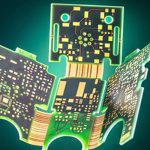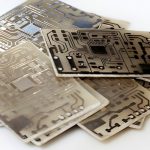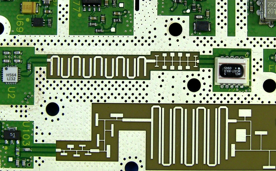
What Is a Teflon PCB?
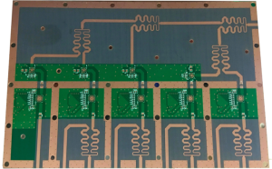
A Teflon PCB is a printed circuit board that uses polytetrafluoroethylene (PTFE)-based laminate as its primary dielectric material. Teflon is a registered trademark associated with PTFE products, while PTFE itself is a fluoropolymer known for its excellent chemical resistance, low friction, low moisture absorption, thermal stability, and outstanding electrical insulation properties.
PTFE is particularly important in high-frequency electronics because of its low dielectric constant (Dk) and low dissipation factor (Df). These characteristics help reduce dielectric loss and signal attenuation, making PTFE-based materials suitable for demanding RF, microwave, radar, telecommunications, and other high-frequency applications.
Unlike conventional FR-4 materials, PTFE laminates are engineered specifically for applications where low dielectric loss and stable electrical performance are critical. Depending on the formulation, PTFE may be reinforced with woven glass, ceramic fillers, or other materials to improve dimensional stability, mechanical strength, thermal performance, and manufacturability.
A PTFE PCB therefore represents more than simply a PCB made from a different substrate. Its material characteristics directly influence impedance control, signal propagation, thermal behavior, fabrication processes, and overall reliability.
Composition of a Teflon PCB
The structure of a PTFE PCB Material system depends on the application and manufacturer, but a typical PTFE-based PCB includes several key components.
PTFE-Based Laminate
PTFE is the primary dielectric material. It provides excellent electrical insulation and low-loss characteristics that are particularly useful for high-frequency signals.
Different PTFE laminate systems can have different Dk, Df, thermal expansion, copper adhesion, and mechanical properties. Therefore, material selection should be based on the actual electrical and mechanical requirements of the design.
Reinforcement and Fillers
PTFE itself has relatively high thermal expansion and can be mechanically softer than conventional rigid PCB laminates. To improve dimensional stability and mechanical properties, manufacturers may use woven glass reinforcement, ceramic fillers, or other engineered materials.
The reinforcement system also affects the effective dielectric constant and the behavior of the finished PCB.
Copper Foil
Copper foil forms the conductive traces, pads, planes, and other electrical structures of the PCB.
For high-frequency applications, copper surface roughness can become an important consideration because conductor loss increases with frequency. Therefore, the selection of copper foil and its surface treatment should be evaluated together with the operating frequency and signal requirements.
Key Properties of Teflon PCB
A Teflon PCB offers several material characteristics that make it suitable for high-frequency and high-performance electronic systems.
Low Dielectric Constant (Dk)
PTFE has a naturally low dielectric constant. Depending on the specific PTFE composite, reinforcement, frequency, and test method, typical Dk values may be around 2.1–2.3 for certain unfilled PTFE systems, while reinforced or filled materials can have significantly different values.
A low Dk can support faster signal propagation and can help designers achieve specific impedance characteristics with appropriate trace geometry.
However, designers should always use the manufacturer’s specified Dk at the relevant frequency rather than relying on a generic PTFE value.
Low Dissipation Factor (Df)
One of the major advantages of PTFE PCB materials is their very low dissipation factor compared with many conventional PCB laminates.
Low Df means less dielectric energy is converted into heat as a high-frequency signal travels through the transmission line. This helps reduce insertion loss and signal attenuation.
The actual Df varies according to the PTFE formulation, reinforcement, filler content, frequency, and test method, so the material datasheet should be used during high-frequency design.
High Thermal Stability
PTFE-based materials can withstand elevated temperatures and maintain useful electrical and mechanical performance over a broad temperature range.
Some PTFE materials have continuous-use temperature ratings around 260°C, but this should not be interpreted as the maximum operating temperature of a complete PCB. The actual thermal capability of the finished board depends on the laminate grade, copper, bonding materials, solder mask, surface finish, components, assembly process, and environmental conditions.
Excellent Chemical Resistance
PTFE is highly resistant to many chemicals, solvents, acids, and other aggressive substances.
This property makes PTFE-based materials attractive for industrial and specialized electronic systems exposed to demanding environments. Nevertheless, the complete PCB assembly must be evaluated because other materials used in the board construction may have different chemical resistance.
Low Moisture Absorption
PTFE has very low moisture absorption compared with many conventional dielectric materials.
Low moisture absorption can help maintain more stable electrical characteristics in humid environments. This can be particularly valuable for RF and microwave circuits where changes in dielectric properties can affect impedance and signal performance.
Stable High-Frequency Performance
The combination of low Dk, low Df, and low moisture absorption makes High Frequency PCB designs based on PTFE particularly attractive for RF and microwave systems.
For demanding applications, designers should evaluate the complete transmission-line structure, including dielectric thickness, copper roughness, trace width, reference planes, connectors, and surface finish.
Advantages of Teflon PCB
Excellent Electrical Performance
The low dielectric loss of PTFE materials makes them well suited to high-frequency and high-speed signal transmission.
A properly designed Teflon PCB can help minimize signal attenuation and maintain signal integrity over demanding transmission paths. This is especially important in RF, microwave, radar, satellite communications, and high-frequency wireless systems.
Low Signal Loss
Signal loss in a high-frequency PCB comes from several sources, including conductor loss, dielectric loss, radiation, and discontinuities.
The low Df of PTFE can significantly reduce dielectric loss compared with higher-loss materials. However, achieving low total insertion loss also requires appropriate copper foil selection, surface roughness control, impedance design, and connector transitions.
High Thermal Reliability
PTFE-based laminates can provide good thermal stability in applications exposed to elevated temperatures.
When combined with appropriate reinforcement and PCB construction, they can support demanding RF and industrial environments where both electrical and thermal stability are required.
Chemical and Moisture Resistance
The chemical resistance and low moisture absorption of PTFE contribute to stable performance in harsh environments.
This makes PTFE-based circuit boards useful for equipment operating in industrial, outdoor, and other environments where moisture and chemical exposure may affect conventional materials.
Long-Term Reliability
When the correct material system and manufacturing process are selected, PTFE-based PCBs can provide reliable performance over extended service periods.
Reliability depends not only on the PTFE dielectric but also on copper adhesion, plated-through-hole construction, thermal cycling, mechanical stress, soldering conditions, and overall PCB design.
Teflon PCB Manufacturing Process
PTFE PCB Manufacturing requires specialized processes because PTFE behaves differently from conventional epoxy-based PCB materials.
PTFE has a relatively low surface energy and different mechanical characteristics from FR-4, which can affect copper adhesion, drilling, hole preparation, plating, and lamination.
A typical manufacturing process includes the following stages.
Material Preparation
The first step is selecting the appropriate PTFE-based laminate.
The laminate may contain woven glass reinforcement, ceramic fillers, or other additives depending on the required Dk, Df, thermal expansion, mechanical strength, and dimensional stability.
Material thickness and copper foil type must be selected according to the required impedance and electrical performance.
Copper Cladding
Copper foil is bonded to the PTFE-based dielectric material to create the copper-clad laminate.
The bonding method depends on the specific laminate construction. Some materials use specially engineered bonding systems, while others use advanced adhesiveless structures.
Because PTFE has low surface energy, achieving reliable copper adhesion requires careful material selection and process control.
Layer Stackup and Lamination
For multilayer PTFE PCB designs, dielectric sheets, copper foils, and bonding layers are arranged according to the specified stackup.
Accurate registration is critical because small dimensional variations can affect controlled impedance and the alignment of high-frequency structures.
Lamination parameters must be carefully controlled according to the material supplier’s recommended process window. Unlike conventional FR-4 processing, PTFE-based materials may require specialized lamination techniques.
Drilling
Mechanical drilling or laser drilling may be used depending on the material construction, hole size, layer count, and design requirements.
PTFE-based materials can present challenges during drilling because of their softness and tendency to deform under mechanical stress.
Proper drill selection, feed rate, spindle speed, tool condition, and process parameters are therefore important to minimize burrs, deformation, and other defects.
Hole Preparation and Metallization
After drilling, the hole walls must be prepared for reliable copper plating.
Because PTFE has low surface energy and excellent chemical resistance, conventional FR-4 desmear processes may not be sufficient. Specialized surface treatment or plasma-based processes may be used to improve hole-wall adhesion.
A thin layer of electroless copper is then deposited onto the prepared hole walls, followed by electroplating when required.
Reliable hole metallization is particularly important in multilayer RF PCB and microwave applications.
Imaging and Etching
A photoresist is applied to the copper surface and exposed according to the required circuit pattern.
After development, unwanted copper is removed through controlled etching, leaving the required traces, pads, transmission lines, and ground structures.
For high-frequency boards, trace width and spacing must be tightly controlled because small geometric changes can influence impedance and signal performance.
Solder Mask and Protective Coatings
A suitable solder mask or protective coating may be applied depending on the PCB design and application.
However, high-frequency circuits require careful consideration of solder mask coverage because the additional dielectric material can affect the effective dielectric environment and therefore influence impedance.
Some RF and microwave designs intentionally leave critical transmission-line structures exposed or use controlled solder mask configurations.
Surface Finish
Exposed copper pads may receive a surface finish such as ENIG, immersion silver, immersion tin, or another appropriate finish.
Surface finish selection should consider solderability, contact requirements, corrosion resistance, high-frequency loss, and manufacturing requirements.
For RF applications, the impact of surface roughness and plated copper characteristics may also need to be considered.
Component Assembly
Components are mounted using the appropriate soldering and assembly process.
High-frequency assemblies require careful control of component placement, solder joints, grounding, and interconnections because even small parasitic effects can influence RF performance.
Testing and Quality Control
Testing is an essential part of PTFE PCB Manufacturing.
Depending on the application, testing and inspection may include:
- Electrical testing: Verifies continuity and isolation and identifies open or short circuits.
- AOI inspection: Checks PCB patterns and visible manufacturing defects.
- Dimensional inspection: Verifies critical board dimensions and layer registration.
- Plated-hole inspection: Evaluates hole quality and metallization.
- Impedance testing: Confirms that controlled-impedance structures meet the specified target.
- Functional testing: Evaluates electrical performance under specified operating conditions.
- RF testing: May be performed for specialized RF and microwave assemblies when required.
Applications of Teflon PCB
The electrical properties of PTFE make Teflon PCB technology particularly useful in applications where low signal loss and stable high-frequency performance are critical.
Telecommunications
Telecommunications systems use high-frequency RF and microwave circuits for wireless communication, signal processing, antennas, and other functions.
A Microwave PCB based on PTFE can provide low dielectric loss and stable electrical performance, making it suitable for high-frequency communication equipment.
Potential applications include base stations, RF modules, antennas, filters, amplifiers, and wireless communication systems.
Automotive Electronics
Modern vehicles increasingly rely on high-frequency electronics for radar, sensing, communication, and advanced driver-assistance systems.
PTFE-based PCBs can be used in automotive radar and other RF circuits where signal integrity and low loss are important.
For example, radar systems operating in the 24 GHz or 77 GHz range require carefully controlled PCB materials and transmission-line structures. PTFE-based high-frequency laminates can be considered when the required electrical performance exceeds the capabilities of conventional FR-4.
Industrial Equipment
Industrial measurement and control systems may require high-frequency signal processing, sensors, instrumentation, and communication circuits.
The low signal loss and environmental resistance of PTFE materials can make them suitable for specialized measurement equipment, RF instrumentation, industrial sensors, and other demanding systems.
Medical Equipment
High-frequency electronics are used in various medical imaging, diagnostic, therapeutic, and monitoring systems.
PTFE-based PCBs may be used in selected RF and microwave circuits where low loss and stable dielectric properties are important.
However, the suitability of PTFE for a specific medical product depends on the complete device architecture, applicable regulatory requirements, material compatibility, and reliability validation. Claims about direct implantation or biological compatibility should be evaluated separately rather than assuming that every PTFE PCB is suitable for implantable medical devices.
Aerospace and Defense
Aerospace and defense systems often require lightweight, stable, and high-performance RF electronics.
PTFE-based RF PCB and microwave laminates can be used in radar, satellite communication, navigation, electronic sensing, and other high-frequency systems.
The low dielectric loss of PTFE can help support efficient signal transmission at microwave and millimeter-wave frequencies.
Challenges of Using Teflon PCB
Although PTFE offers excellent electrical characteristics, manufacturing a Teflon PCB can be more challenging than manufacturing a conventional FR-4 PCB.
Difficult Material Processing
PTFE has different mechanical and surface characteristics from epoxy-based laminates.
These differences affect drilling, surface preparation, copper adhesion, plating, and lamination. Specialized processes and experienced operators are often required to achieve consistent manufacturing results.
Copper Adhesion
The low surface energy of PTFE can make copper adhesion more difficult than with conventional PCB materials.
The laminate and bonding system must therefore be selected carefully, and appropriate surface treatment and manufacturing processes must be used.
Higher Material Cost
PTFE-based high-frequency laminates are generally more expensive than standard FR-4 materials.
The total PCB cost can also increase because of specialized processing, tighter process controls, material handling requirements, and additional testing.
Manufacturing Complexity
Multilayer PTFE boards can require specialized lamination, drilling, plating, and registration processes.
Manufacturers without sufficient experience in high-frequency materials may encounter difficulties maintaining dimensional accuracy, plated-hole reliability, and consistent electrical performance.
Design Complexity
High-frequency PCB design requires careful control of many parameters, including:
- Dielectric thickness.
- Dk and Df.
- Trace width and spacing.
- Copper thickness and roughness.
- Reference-plane structure.
- Via transitions.
- Connector geometry.
- Solder mask configuration.
- Stackup tolerances.
- Thermal expansion.
Therefore, electrical simulation and impedance calculations should be incorporated into the design process when appropriate.
Thermal Management
Although PTFE itself offers good thermal stability, the thermal conductivity of a particular PTFE laminate can vary significantly depending on reinforcement and filler composition.
High-power RF circuits may generate considerable heat, so thermal management should be evaluated at the system level. Copper planes, thermal vias, heatsinks, substrate selection, and component placement may all contribute to thermal performance.
Maintaining Signal Integrity
At high frequencies, small variations in trace geometry, dielectric thickness, copper roughness, connectors, and vias can affect signal integrity.
For this reason, High Frequency PCB designs require tighter control than many conventional digital PCB applications.
Key Design Considerations for PTFE PCB
Before starting PTFE PCB Manufacturing, engineers should consider both electrical and manufacturing requirements.
Material Selection
Do not select a PTFE laminate only because it has a low nominal Dk.
The material should be evaluated according to:
- Dk at the target frequency.
- Df at the target frequency.
- Dielectric thickness.
- Thermal expansion.
- Thermal conductivity.
- Copper adhesion.
- Reinforcement structure.
- Mechanical stability.
- Manufacturing compatibility.
Controlled Impedance
RF and microwave transmission lines often require tightly controlled impedance.
The target impedance depends on the application and interface. Common single-ended designs may use 50 Ω, while differential systems may use other specified impedance values.
Trace width, copper thickness, dielectric thickness, Dk, reference-plane spacing, and manufacturing tolerances all affect the final impedance.
Copper Surface Roughness
At high frequencies, current tends to concentrate near the conductor surface due to the skin effect.
As frequency increases, copper surface roughness can contribute more significantly to conductor loss. Low-profile or specially treated copper may therefore be preferred for some low-loss high-frequency applications.
Thermal Expansion
PTFE-based materials can have relatively high thermal expansion compared with conventional PCB materials, particularly in the Z-axis.
For multilayer boards with plated through-holes, thermal expansion should be considered carefully because repeated thermal cycling can place mechanical stress on plated copper.
Mechanical Handling
PTFE laminates may be softer and more easily deformed than FR-4.
Careful handling during drilling, routing, lamination, and assembly is therefore important to prevent mechanical damage and dimensional variation.
Why Choose Kingda for Teflon PCB Manufacturing?
Selecting an experienced PTFE PCB Manufacturing partner is important when working with high-frequency materials.
Kingda provides customized PCB manufacturing and engineering support for applications requiring specialized materials and high-frequency performance.
High-Frequency PCB Expertise
PTFE-based PCB manufacturing requires different processing considerations from conventional FR-4 production. Kingda can evaluate material selection, stackup requirements, impedance specifications, and manufacturing constraints according to the customer’s application.
Engineering Support
Kingda can assist with reviewing PCB fabrication data and identifying potential manufacturing challenges related to layer registration, drilling, plating, trace geometry, material selection, and controlled impedance.
Quality-Focused Manufacturing
High-frequency PCBs require consistent control of critical dimensions and material properties. Kingda emphasizes process control and inspection throughout PCB production to support reliable and repeatable results.
Customized Solutions
Different RF, microwave, telecommunications, automotive, industrial, and aerospace applications can require different PTFE laminate systems and PCB structures.
Kingda can work with customers to develop customized PCB solutions based on electrical, mechanical, thermal, and manufacturing requirements.
From Prototype to Production
Whether the project requires prototype development or volume production, early communication between the PCB designer and manufacturer can help identify material and process issues before manufacturing begins.
Kingda can support customers through PCB fabrication, inspection, testing, and production coordination.
Conclusion
A Teflon PCB is a specialized high-frequency circuit board that uses PTFE-based dielectric materials to achieve low dielectric loss, stable electrical performance, low moisture absorption, and excellent chemical resistance.
These characteristics make PTFE PCB technology particularly valuable for telecommunications, RF and microwave systems, automotive radar, industrial electronics, medical equipment, aerospace, and other high-performance applications.
However, PTFE PCB technology also presents manufacturing and design challenges. Copper adhesion, drilling, plating, lamination, thermal expansion, material cost, impedance control, and signal integrity require careful consideration.
For demanding high-frequency applications, the best results come from selecting the appropriate PTFE laminate, designing the complete transmission-line structure correctly, and working with a manufacturer experienced in specialized high-frequency PCB fabrication.
Kingda can provide customized PCB manufacturing and engineering support to help customers develop reliable PTFE-based circuit board solutions according to their specific electrical and mechanical requirements.