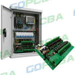
What Is a 4-Layer PCB?
As electronic technology continues to advance, modern electronic products are becoming smaller, faster, and more functionally integrated. This development has increased the demand for printed circuit boards with higher routing density, better electrical performance, and greater design flexibility.
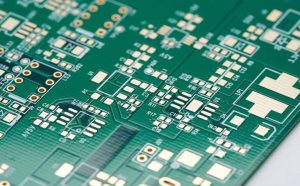
A 4-Layer PCB is a multilayer printed circuit board consisting of four conductive copper layers separated by dielectric materials. These layers are laminated together under controlled temperature and pressure to form a single rigid circuit board.
Unlike a two-layer PCB, a four-layer board provides additional internal layers that can be used for signal routing, power distribution, or ground planes. This makes it possible to achieve higher circuit density, improved signal integrity, better electromagnetic compatibility, and more organized power distribution.
A typical four-layer PCB can contain two outer signal layers and two inner layers dedicated to ground, power, or additional signal routing. The exact arrangement depends on the electrical requirements, component density, mechanical constraints, and manufacturing capabilities of the project.
Because it provides a practical balance between performance, complexity, and cost, the 4-Layer PCB is one of the most widely used multilayer PCB configurations.
What Is a 4-Layer PCB Stackup?
A PCB Stackup defines the order of copper layers and dielectric materials within a multilayer circuit board.
In a four-layer PCB, there are four copper layers, commonly identified as L1, L2, L3, and L4. Between these copper layers are dielectric materials such as core and prepreg.
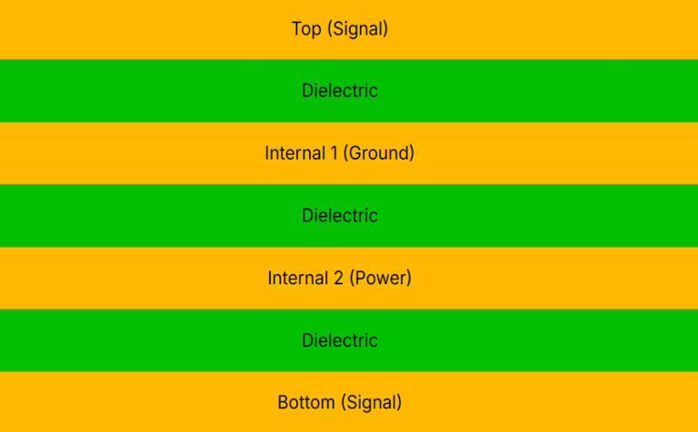
A simplified four-layer structure may look like this:
Layer 1 — Signal
Layer 2 — Ground
Layer 3 — Power
Layer 4 — Signal
However, this is only one possible arrangement. The optimal 4-Layer PCB Stackup depends on signal speed, impedance requirements, power distribution, EMI performance, manufacturing cost, and component placement.
Signal – Ground – Power – Signal
This is one of the most common four-layer configurations.
The outer layers are primarily used for signal routing, while the inner layers provide dedicated ground and power planes.
This arrangement provides several benefits:
- Convenient power distribution
- A relatively continuous ground reference
- Shorter return-current paths
- Good support for controlled-impedance routing
- Improved electromagnetic performance
- Straightforward PCB fabrication
High-speed signals can be routed on the outer signal layers with the adjacent ground plane serving as a reference.
However, designers should pay attention to the dielectric thickness between the signal and reference layers because it directly affects controlled impedance.
Signal – Ground – Ground – Signal
Another useful configuration is:
Layer 1 — Signal
Layer 2 — Ground
Layer 3 — Ground
Layer 4 — Signal
This stackup provides strong ground referencing for both outer signal layers.
It can be useful when signal integrity and electromagnetic performance are more important than having a dedicated internal power plane.
One limitation is that power distribution must be implemented through traces or copper pours on available layers rather than through a dedicated power plane.
This configuration can work well for compact communication devices, networking equipment, GPS-related circuits, and other designs where controlled impedance and low-noise signal transmission are important.
Signal – Ground – Signal – Ground
Another possible configuration is:
Layer 1 — Signal
Layer 2 — Ground
Layer 3 — Signal
Layer 4 — Ground
This arrangement provides a ground reference adjacent to each signal layer.
It can be considered for designs containing noise-sensitive signals or applications where electromagnetic compatibility is an important concern.
However, it does not always provide the most efficient power distribution structure. Designers should therefore evaluate the power requirements before selecting this stackup.
Signal – Power – Power – Signal
In some designs, the two internal layers can be used primarily for power distribution:
Layer 1 — Signal
Layer 2 — Power
Layer 3 — Power
Layer 4 — Signal
This structure may be useful when a product requires multiple supply voltages.
Different power regions can be allocated within the internal copper layers, although careful partitioning is necessary to avoid creating undesirable return-current paths or increasing coupling between power domains.
Ground can be distributed through copper pours or dedicated routing regions on the signal layers.
Core and Prepreg in a 4-Layer PCB
A multilayer PCB typically uses two primary dielectric structures: core and prepreg.
The core is a rigid laminate with copper foil already bonded to one or both sides. Prepreg is a resin-impregnated glass-fiber material used to bond PCB layers together during lamination.
During manufacturing, heat and pressure cause the resin in the prepreg to flow and cure, creating a mechanically stable multilayer structure.
The selection of core and prepreg materials affects:
- Layer-to-layer spacing
- Controlled impedance
- Dielectric thickness
- Thermal performance
- Mechanical stability
- Manufacturing cost
- Signal integrity
For high-speed designs, dielectric thickness and dielectric constant should be carefully controlled because they directly affect trace impedance and signal propagation.
Using multiple core materials may provide greater flexibility in stackup design, but it can also increase manufacturing complexity and cost.
Advantages of 4-Layer PCBs
The 4-Layer PCB is widely used because it offers a strong balance between design flexibility and manufacturing cost.
Higher Routing Density
A four-layer PCB provides twice the conductive layer count of a conventional two-layer PCB.
This additional routing space allows engineers to accommodate more connections without significantly increasing board dimensions.
Components can be placed more densely while maintaining practical routing channels.
Better Signal Integrity
One of the major benefits of a well-designed four-layer board is improved Signal Integrity.
A dedicated ground plane can provide a stable reference for high-speed signals and help reduce the size of current loops.
When the stackup is properly designed, the board can provide:
- More predictable impedance
- Better return-current paths
- Reduced signal reflections
- Lower crosstalk
- Improved electromagnetic compatibility
However, simply increasing the number of PCB layers does not automatically guarantee better signal integrity. The layer arrangement, dielectric thickness, trace geometry, and grounding strategy must all be properly designed.
Support for Impedance Control
A four-layer structure is well suited for Impedance Control.
Controlled impedance is particularly important for high-speed interfaces and communication signals.
The characteristic impedance of a PCB trace is influenced by factors including:
- Trace width
- Copper thickness
- Dielectric thickness
- Dielectric constant
- Distance to the reference plane
A suitable four-layer stackup can therefore make it easier to achieve the required single-ended and differential impedance.
Better Power and Ground Distribution
Internal copper planes can be used to distribute power and ground more efficiently.
A dedicated ground plane can provide a low-impedance return path, while a power plane or copper region can distribute supply voltage to multiple components.
This can simplify routing and reduce the need for long power traces.
Better Thermal Performance
Additional copper layers can also contribute to thermal management.
Copper planes can spread heat over a larger area and transfer heat toward other parts of the PCB.
For higher-power applications, thermal vias, larger copper areas, heavier copper, heatsinks, or other thermal solutions may be required.
Improved Mechanical Strength
The additional copper and dielectric layers can increase the overall mechanical stability of the PCB.
A properly laminated four-layer board generally provides good dimensional stability and resistance to mechanical deformation.
Good Balance Between Cost and Performance
Compared with six-layer or higher-layer-count PCBs, four-layer boards can provide many advanced design capabilities at a lower manufacturing cost.
This makes them particularly attractive for products requiring moderate-to-high circuit density without the need for a more complex multilayer structure.
Factors Affecting 4-Layer PCB Cost
The cost of a 4-Layer PCB depends on more than simply the number of layers.
Impedance Control
Controlled impedance can increase manufacturing costs because it requires tighter control of trace geometry, dielectric thickness, copper thickness, and material properties.
Manufacturers may also need to perform additional testing and verification to confirm that the finished board meets the required impedance specifications.
PCB Stackup
The selected PCB Stackup has a direct influence on material usage and manufacturing complexity.
Different combinations of core and prepreg materials can result in different costs.
A stackup using multiple core materials or specialized high-frequency laminates may cost more than a standard FR-4 structure.
Advanced PCB Technologies
Advanced technologies such as HDI, microvias, blind vias, buried vias, fine-pitch features, and sequential lamination can significantly increase the cost of a four-layer board.
These technologies should therefore be used only when they provide a clear technical benefit.
Copper Weight
Copper thickness is another important cost factor.
Higher copper weight increases material consumption and may require additional manufacturing considerations.
The appropriate copper thickness depends on:
- Current requirements
- Trace width
- Thermal requirements
- Power distribution
- Mechanical requirements
Heavy-copper construction can be beneficial for high-current applications but generally increases production cost.
Board Size and Shape
Larger boards consume more raw materials and may reduce the number of panels that can be produced from a standard production sheet.
Unusual board shapes can also increase material waste and manufacturing complexity.
Surface Finish
The selected PCB Surface Finish also affects the final price.
Common options include HASL, lead-free HASL, ENIG, OSP, immersion tin, and immersion silver.
The best finish depends on assembly requirements, component technology, storage conditions, reliability requirements, and budget.
Production Quantity
Production volume has a significant effect on unit cost.
Prototype and small-batch production typically have higher unit costs, while larger production volumes allow manufacturers to optimize material utilization and production efficiency.
4-Layer PCB Manufacturing Process
The PCB Manufacturing process for a four-layer board is more complex than the process used for single- or double-sided PCBs.
Although the exact process varies between manufacturers, the major stages typically include the following.
1. PCB Design and Engineering Review
The process begins with schematic design and PCB layout.
Engineers define the layer stackup, component placement, signal routing, power distribution, ground planes, impedance requirements, and mechanical dimensions.
A DFM review is recommended before fabrication to identify potential manufacturing issues.
2. Material Preparation
The manufacturer selects the appropriate core, copper foil, and prepreg materials.
The material selection is based on electrical performance, thermal requirements, mechanical properties, operating environment, and cost.
For standard applications, FR-4 is widely used. High-frequency or high-speed applications may require specialized low-loss laminate materials.
3. Inner-Layer Circuit Formation
The internal copper layers are patterned using imaging and etching processes.
The desired signal, power, and ground structures are transferred onto the copper surfaces.
After etching, the inner layers are inspected to verify the circuit pattern.
4. Inner-Layer Inspection
Automated Optical Inspection (AOI) can be used to identify defects such as:
- Missing copper
- Excess copper
- Short circuits
- Open circuits
- Pattern deviations
- Foreign material
This inspection is important because internal-layer defects become difficult to access after lamination.
5. Lamination
The inner layers, core materials, copper foils, and prepreg are carefully stacked according to the designed PCB Stackup.
The stack is then laminated under controlled temperature and pressure.
During this process, the resin in the prepreg flows and cures, bonding the individual layers into one solid multilayer PCB.
Precise control of temperature, pressure, resin flow, and alignment is essential.
6. Drilling
After lamination, holes are drilled according to the fabrication data.
These holes can include:
- Plated through-holes
- Component holes
- Mounting holes
- Other mechanical openings
Drilling accuracy is critical because the holes must connect the correct internal copper layers.
7. Hole Preparation and Copper Plating
After drilling, the hole walls are cleaned and prepared for plating.
A conductive copper layer is deposited onto the hole walls, followed by copper plating to achieve the required thickness.
This creates reliable electrical connections between the external layers and internal copper layers.
8. Outer-Layer Imaging and Etching
The outer copper layers are patterned according to the PCB design.
The required traces, pads, and other conductive features are formed through imaging, plating, and etching processes.
9. Solder Mask Application
A solder mask is applied to both outer surfaces of the PCB.
The solder mask protects the copper circuitry and leaves designated pads exposed for component soldering.
10. Surface Finish
The exposed copper pads receive the selected surface finish.
The finish protects copper from oxidation and improves solderability during assembly.
11. Silkscreen Printing
Component reference designators, polarity markings, product information, logos, and other markings are printed onto the board.
12. Electrical Testing and Final Inspection
The finished four-layer PCB undergoes electrical and visual inspection.
Depending on the application, testing may include:
- AOI
- Flying probe testing
- In-circuit testing
- Open and short testing
- Dimensional inspection
- Solderability testing
- Impedance testing
The final inspection verifies that the finished board meets the customer’s electrical, mechanical, and visual requirements.
Design Considerations for 4-Layer PCBs
Selecting an appropriate stackup is one of the most important decisions when designing a four-layer PCB.
Keep High-Speed Signals Close to a Reference Plane
High-speed traces should generally be routed close to a continuous reference plane.
This helps provide a predictable return-current path and reduces loop area.
Avoid Splitting the Reference Plane Under Critical Signals
Critical high-speed traces should not cross gaps or discontinuities in their reference plane unless the return-current path is properly addressed.
An interrupted reference plane can increase electromagnetic radiation and cause signal-integrity problems.
Control Trace Impedance
When impedance-controlled routing is required, trace width, dielectric thickness, copper thickness, and laminate characteristics should be defined together.
Designers should work with the PCB manufacturer early in the process to ensure that the proposed stackup can achieve the required impedance.
Separate Sensitive Signals
Analog, digital, power, and high-speed signals may need careful placement and routing to reduce unwanted coupling.
However, signal partitioning should be based on actual current-return behavior rather than simply dividing the board into isolated areas.
Use Ground Planes Effectively
A continuous ground plane can provide a low-impedance return path and improve electromagnetic performance.
It can also reduce the need for long ground traces and simplify the routing of many circuits.
4-Layer PCB Applications
Four-layer boards are suitable for many electronic products that require moderate circuit density and improved electrical performance.
Typical PCB Applications include:
- Industrial control equipment
- Automotive electronics
- Communication equipment
- Networking devices
- Power management systems
- Consumer electronics
- Medical electronics
- Embedded systems
- IoT devices
- Motor controllers
- Instrumentation equipment
- Security systems
- LED control systems
For products requiring very high routing density, multiple voltage domains, advanced high-speed interfaces, or extensive RF functionality, a six-layer or higher-layer-count PCB may be more appropriate.
Why Choose Kingda for 4-Layer PCB Manufacturing?
Choosing an experienced PCB manufacturer is essential when manufacturing four-layer boards because multilayer fabrication requires accurate layer alignment, controlled lamination, reliable plating, and consistent material properties.
Kingda provides professional PCB Manufacturing services for four-layer boards and other PCB technologies.
Reliable Manufacturing Quality
Kingda uses controlled production processes and inspection procedures to maintain consistent quality throughout multilayer PCB manufacturing.
Competitive Pricing
Through optimized material usage, efficient production processes, and experienced engineering management, Kingda works to provide competitive pricing without compromising essential quality requirements.
Professional Engineering Support
Kingda can assist customers with stackup selection, DFM review, material selection, impedance requirements, and manufacturing optimization.
Early engineering communication can help identify potential problems before production and reduce unnecessary manufacturing costs.
Flexible Production Capability
Four-layer PCBs can be produced for prototypes, small batches, and volume production according to project requirements.
Strict Quality Control
Multilayer PCB manufacturing requires precise control of layer alignment, lamination, drilling, plating, and electrical performance. Kingda applies inspection and testing procedures throughout the production process.
One-Stop PCB Manufacturing
Kingda provides integrated PCB manufacturing support, helping customers manage design-for-manufacturing requirements, fabrication, testing, and production more efficiently.
Conclusion
A 4-Layer PCB provides an excellent balance between circuit density, electrical performance, manufacturing complexity, and cost.
By using four copper layers, designers can create dedicated ground and power structures while retaining additional routing space for signal traces. A carefully designed 4-Layer PCB Stackup can also improve Signal Integrity, support Impedance Control, simplify power distribution, and improve overall electromagnetic performance.
However, the number of layers alone does not determine PCB performance. Stackup design, dielectric thickness, trace geometry, grounding, material selection, copper weight, and manufacturing quality all play important roles.
For applications that are too complex for a two-layer PCB but do not require the additional cost of a six-layer or higher-layer board, a four-layer PCB is often an efficient and reliable solution.