What Is an Embedded PCB?
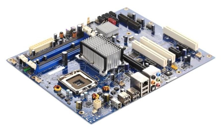
An Embedded PCB is a printed circuit board in which active or passive electronic components are integrated into the internal structure of the board rather than being mounted exclusively on its outer surfaces.
Traditional PCB assembly typically places components on the top or bottom surface using through-hole technology (THT) or surface-mount technology (SMT). In contrast, embedded technology allows selected components to be placed inside the PCB stackup or manufactured directly into the internal circuit structure.
Common Embedded Components include resistors, capacitors, inductors, and, in some advanced applications, semiconductor devices.
This approach is sometimes referred to as embedded component technology, embedded PCB technology, or 3D PCB integration because it uses the internal volume of the PCB to achieve greater circuit integration.
By moving components into the PCB structure, designers can shorten electrical interconnections, reduce parasitic effects, improve signal integrity, save surface area, and create thinner and more compact electronic products.
Embedded PCB technology is particularly useful for high-density electronics, miniaturized devices, high-speed circuits, power electronics, automotive systems, telecommunications equipment, medical devices, and other applications where board space and electrical performance are critical.
Advantages of Embedded PCBs
The use of an Embedded PCB can provide several electrical, mechanical, thermal, and manufacturing benefits.
PCB Miniaturization
Embedding components inside the PCB reduces the number of components that must occupy the outer surfaces.
This can free valuable space for connectors, larger components, antennas, heat-dissipation structures, and other functional elements. It is especially useful for compact electronic products where PCB area is limited.
Shorter Electrical Interconnections
Conventional surface-mounted components may require relatively long traces between components.
With Embedded Components, the electrical distance can be significantly reduced. Shorter connections can lower parasitic inductance and capacitance, reduce transmission loss, and improve high-frequency performance.
Improved Signal Integrity
Shorter interconnects can help reduce unwanted inductance, electromagnetic coupling, and signal reflection.
For high-speed designs, embedding components closer to the IC or signal path can improve signal integrity and help designers achieve more predictable electrical behavior.
Higher Component Density
Components can be distributed through the internal layers rather than being limited to the top and bottom surfaces.
This provides greater freedom for high-density circuit design and can increase functional density without significantly increasing the external PCB footprint.
Improved Reliability
Removing external solder joints and reducing the length of interconnections can potentially improve mechanical reliability.
Embedded components are protected by the surrounding PCB structure, which can reduce their exposure to mechanical impact, contamination, and environmental conditions.
Better Thermal Management
Certain embedded structures can improve heat transfer by creating shorter thermal paths or integrating thermally conductive materials into the PCB.
This is particularly useful for power electronics and high-current applications where heat dissipation is a major design consideration.
More Functional Surface Area
When selected components are embedded inside the board, additional space becomes available on the outer layers.
This can make it easier to place connectors, sensors, antennas, shielding structures, and other components.
THT, SMT, and Embedded Components Compared
Before examining embedded PCB technology in detail, it is useful to understand how component integration has evolved from conventional through-hole assembly to surface mounting and finally to embedded technology.
| Feature | THT | SMT/SMD | Embedded Components |
|---|---|---|---|
| Mounting position | Through PCB holes | PCB surface | Inside PCB or on PCB surface |
| Interconnection | Component leads through plated holes | Soldered directly to surface pads | Internal or surface interconnection |
| Component density | Relatively low | High | Very high |
| PCB footprint | Large | Smaller | Further reduced |
| Double-sided assembly | Limited by component structure | Fully supported | Supported with internal integration |
| Mechanical protection | Good | Good | Very good for embedded parts |
| Component replacement | Relatively easy | Relatively easy | Difficult after PCB fabrication |
| Typical use | Power, mechanical, legacy circuits | Most modern electronics | High-density and miniaturized electronics |
THT remains useful when strong mechanical connections or high-current components are required. SMT provides much higher placement density and is now the dominant assembly method for many electronic products.
Embedded technology goes one step further by using the internal PCB structure as part of the component integration strategy.
How Are Embedded PCBs Manufactured?
An Embedded PCB can generally be produced using two major approaches:
- Manufacturing passive components directly within the PCB structure.
- Placing discrete components inside cavities formed within the PCB.
The appropriate method depends on the component type, electrical requirements, PCB stackup, component dimensions, thermal requirements, and manufacturing capabilities.
Methods for Manufacturing Embedded PCBs
1. Component Formation Within the PCB
Some passive components can be formed directly during PCB fabrication.
This approach eliminates the need to install a conventional discrete component on the surface.
Embedded Resistors
Embedded Resistors are passive components integrated directly into the PCB structure.
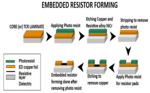
A resistive material can be combined with copper and patterned using processes similar to those used for circuit formation. Depending on the required resistance range and manufacturing technology, thin-film or thick-film resistive materials may be used.
A typical process may involve:
- Applying the resistive material.
- Forming the required circuit pattern.
- Photolithography and exposure.
- Etching or selective removal.
- Stripping the remaining resist.
- Testing and verifying the resistance value.
The final structure functions as an integrated resistor rather than a separately mounted component.
Thin-film technology can provide high resistance precision and fine geometries, while thick-film technology can be advantageous for certain power and manufacturing requirements.
Embedded Inductors
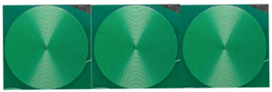
Embedded Inductors can be formed by creating spiral, square, or other winding structures within one or multiple PCB layers.
For example, a multilayer PCB can use a spiral copper pattern to create an inductive structure. Multiple layers may be interconnected through vias to increase the effective inductance.
The performance of an embedded inductor depends on:
- Number of turns
- Trace width
- Trace spacing
- Copper thickness
- Core material
- Magnetic properties
- Distance between layers
- Operating frequency
Embedded inductors can be useful in RF circuits, filters, power converters, and other space-constrained applications.
Embedded Capacitors
Embedded Capacitors are formed by placing a dielectric layer between conductive electrodes within the PCB stackup.
The basic structure is similar to a sandwich:
Copper electrode → dielectric material → copper electrode
The capacitance depends primarily on electrode area, dielectric thickness, and dielectric constant.
Advanced embedded capacitor structures can use high-k dielectric materials to obtain higher capacitance density without requiring a large external capacitor.
A simplified manufacturing sequence includes:
- Formation of the bottom electrode.
- Deposition or lamination of the dielectric layer.
- Formation of the top electrode.
- Patterning and interconnection.
- Electrical testing.
Embedded capacitors can be particularly useful for local power decoupling because the physical distance between the capacitor and the IC power connection can be very short.
2. Placement of Components Inside the PCB Core
Another approach is to install discrete Embedded Components inside cavities formed within the PCB.
The basic process includes:
- Designing the component cavity.
- Defining adequate clearance around the component.
- Fabricating the required PCB layers.
- Forming the cavity.
- Placing the component.
- Securing and electrically connecting the component.
- Completing the remaining lamination or PCB fabrication processes.
- Performing electrical and dimensional inspection.
Cavity dimensions must be carefully controlled because insufficient clearance can create mechanical stress, while excessive clearance can affect lamination quality and registration.
The cavity structure should therefore be considered during PCB layout and DFM analysis rather than being added after the design is completed.
Embedding ICs
In advanced applications, semiconductor devices can also be integrated into internal PCB structures.
The process is considerably more complex than embedding passive components because the design must account for:
- Die dimensions
- Electrical connections
- Thermal paths
- Mechanical stress
- Encapsulation
- CTE mismatch
- Manufacturing tolerances
- Inspection and testing
Since internally embedded components are difficult or impossible to replace after fabrication, component reliability and process control are particularly important.
Embedded Copper Coin PCB
An Embedded Copper Coin PCB integrates a solid copper coin or high-thermal-conductivity copper structure into the PCB to improve heat dissipation.
Copper has excellent thermal conductivity, allowing heat generated by high-power components to move away from localized hot spots more efficiently.
Embedded copper structures can be combined with:
- Thermal vias
- Copper planes
- Heat spreaders
- Thermal interface materials
- Heat sinks
- Copper-filled structures
The appropriate thermal solution depends on component power, heat density, PCB thickness, available space, and the required thermal resistance.
Types of Embedded Copper Coin PCBs
1. Buried Copper Coin PCB
A buried copper coin is installed inside the PCB structure and is not directly visible from the outer surface.
Heat generated near a high-power component can be transferred through thermal vias or thermally conductive structures to the embedded copper coin.
The copper then spreads the heat across a larger area, reducing localized thermal concentration.
This approach is suitable when strong thermal performance is required while maintaining a conventional outer PCB surface.
2. Embedded Copper Coin PCB
In an embedded copper coin structure, a cavity is formed within the PCB and the copper coin is inserted into the designated location.
After the copper structure is secured, it provides a low-resistance thermal path from the heat-generating component toward the desired heat-dissipation area.
The copper coin can be positioned according to the PCB stackup and thermal requirements. Its dimensions, thickness, position, and connection to copper planes must be carefully designed.
Design Considerations for Embedded PCBs
Designing an Embedded PCB requires more than simply deciding where to place a component.
Component Selection
Not every component is suitable for embedding.
Designers should consider:
- Component dimensions
- Operating temperature
- Electrical characteristics
- Reliability requirements
- Moisture sensitivity
- Mechanical strength
- Thermal performance
- Manufacturing compatibility
Components that may require frequent replacement or adjustment are generally poor candidates for embedding.
Cavity Design
For discrete component embedding, cavity dimensions must provide sufficient clearance while maintaining mechanical stability.
The cavity should be considered during stackup design and DFM review.
Electrical Connections
The connection between the embedded component and surrounding copper structure must have low electrical resistance and sufficient mechanical reliability.
For high-frequency applications, parasitic inductance and capacitance should also be included in the design analysis.
Thermal Management
Power components may require dedicated thermal paths.
Copper planes, thermal vias, copper coins, and thermally conductive materials can be combined to transfer heat efficiently.
Reliability
Embedded components cannot normally be replaced easily after PCB fabrication.
Therefore, component quality, lamination reliability, material compatibility, thermal cycling, and electrical testing become especially important.
Manufacturing Tolerances
Embedded structures require tighter dimensional control than many conventional PCB designs.
Designers should work with the manufacturer to define:
- Cavity tolerances
- Component placement tolerances
- Layer registration
- Copper thickness
- Dielectric thickness
- Via dimensions
- Clearance requirements
Early DFM evaluation can prevent manufacturing problems and reduce unnecessary production costs.
Applications of Embedded PCBs
Embedded PCB technology is particularly valuable where space, electrical performance, reliability, or thermal management is critical.
Typical applications include:
- Smartphones and wearable devices
- High-density computing equipment
- Automotive electronics
- Industrial control systems
- Medical devices
- Telecommunications equipment
- IoT products
- RF and microwave circuits
- Power electronics
- Aerospace electronics
- High-speed networking equipment
- Miniaturized consumer electronics
For high-frequency applications, embedded capacitors and inductors can reduce interconnection length and parasitic effects. For power applications, embedded copper structures can provide improved thermal paths.
Why Choose Kingda for Embedded PCB Manufacturing?
Embedded PCB production requires close coordination between circuit design, material selection, component integration, lamination, machining, plating, inspection, and testing.
Kingda provides PCB manufacturing support for projects involving complex multilayer structures and high-density interconnection requirements. Our engineering team can evaluate embedded component requirements together with the PCB stackup, manufacturing process, thermal structure, and DFM considerations.
When selecting an Embedded PCB manufacturing partner, important factors include:
- Experience with complex multilayer PCB structures.
- Engineering support during the design stage.
- Precise cavity and layer-registration control.
- Stable lamination and plating processes.
- Support for embedded passive components.
- Thermal-management solutions.
- Electrical and visual inspection.
- DFM analysis before production.
- Flexible prototype and production support.
- Reliable quality and delivery management.
Kingda can help customers evaluate the appropriate embedded technology based on component type, board structure, electrical performance, thermal requirements, and production objectives.
Conclusion
An Embedded PCB integrates selected active or passive components into the internal PCB structure, creating a more compact and highly integrated electronic platform.
Compared with conventional THT and SMT approaches, embedded technology can reduce interconnection length, increase component density, improve signal integrity, free surface area, and enhance certain thermal and reliability characteristics.
Technologies such as Embedded Resistors, Embedded Capacitors, Embedded Inductors, and Embedded Copper Coin PCB structures provide designers with additional options for miniaturized, high-speed, and high-power electronic systems.
However, embedded PCB technology also introduces greater design and manufacturing complexity. Component selection, cavity dimensions, material compatibility, thermal management, layer registration, electrical connections, and DFM must all be considered before fabrication.
With appropriate design analysis and controlled PCB Manufacturing processes, embedded technology can provide an effective solution for next-generation electronic products that demand higher integration, smaller form factors, and improved electrical and thermal performance.