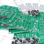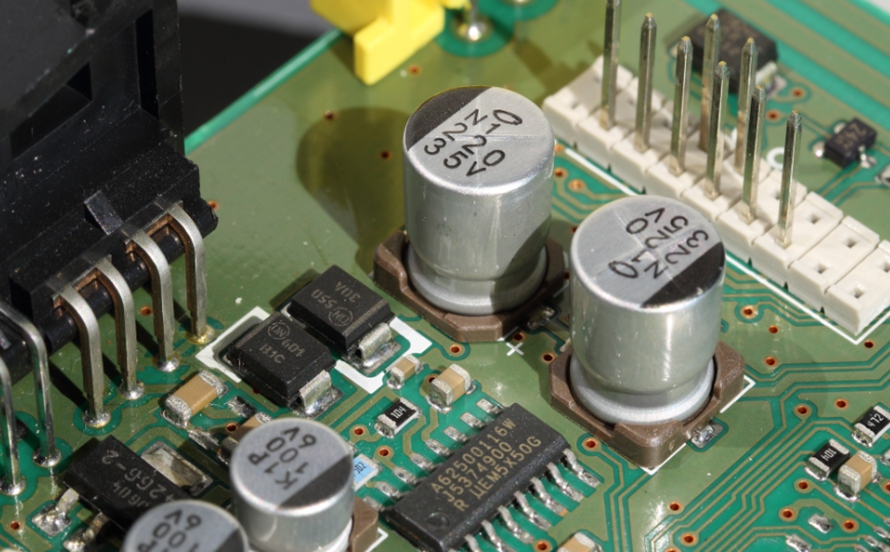
Prototype PCB Assembly is the process of producing a limited number of assembled printed circuit boards to verify a product design before moving into larger-scale production. It allows engineers to evaluate whether the PCB design, components, assembly process, and electrical functions work as intended under practical manufacturing conditions.
During prototyping, engineers may discover design errors, component compatibility problems, layout limitations, thermal issues, or manufacturing constraints that were not obvious during schematic and PCB design. These findings can then be used to modify the circuit, replace components, adjust component placement, improve routing, or revise the manufacturing process.
A well-planned PCB Prototype can therefore reduce development risk, improve product reliability, and provide valuable manufacturing feedback before significant resources are committed to mass production.
At Kingda, prototype assembly can be used as an important step between PCB design and production manufacturing. By evaluating the prototype at both the electrical and manufacturing levels, engineering teams can identify potential problems early and improve the design before production quantities increase.
What Is Prototype PCB Assembly?
Prototype PCB Assembly refers to the manufacturing and assembly of a small number of PCBs for design verification, engineering validation, functional testing, and manufacturing evaluation.
Unlike mass production, where the primary goal is repeatable high-volume manufacturing, prototype assembly focuses on learning and validation.
A prototype can help answer questions such as:
- Does the PCB function according to the schematic?
- Are the selected components suitable for the application?
- Can the components be assembled consistently?
- Are there PCB layout or routing problems?
- Is the soldering process stable?
- Are there thermal or mechanical concerns?
- Can the design be manufactured efficiently?
- Does the product meet its electrical and functional requirements?
The prototype stage is particularly valuable when a product contains complex components, fine-pitch packages, BGA devices, high-speed signals, power electronics, or mixed SMT and through-hole components.
Benefits of Prototype PCB Assembly
Performing PCB Assembly before full-scale production provides several important advantages.
Reduce Development and Manufacturing Costs
Moving directly from a new design to mass production can be expensive if the design contains hidden problems.
A small prototype build allows manufacturers and engineers to identify issues before thousands of boards are produced. Problems such as incorrect component footprints, insufficient clearances, poor solderability, thermal problems, or routing errors can be corrected at a much lower cost.
Early validation can help avoid:
- Large-scale production scrap
- Expensive redesigns
- Product recalls
- Repeated manufacturing cycles
- Excessive engineering analysis
- Delayed product launches
The purpose of prototyping is not simply to produce a small number of boards. It is to reduce the technical and financial risks associated with the next stage of production.
Improve Product Understanding
Prototype manufacturing creates an opportunity for designers, engineers, and manufacturing teams to evaluate the product together.
Some issues only become apparent when a design is physically manufactured. For example, a component may be difficult to place, a connector may interfere with a mechanical enclosure, or a high-power component may generate more heat than expected.
The information collected during prototyping can then be used to improve the next design revision.
Improve Quality
Early prototypes allow potential defects to be identified before the product enters volume manufacturing.
Engineers can evaluate solder joints, component placement, electrical performance, thermal behavior, mechanical fit, and other characteristics.
The prototype stage can therefore become an important part of the product quality strategy rather than simply a preliminary manufacturing step.
Accelerate Design Iteration
Prototype builds provide physical feedback much faster than relying entirely on theoretical simulation.
Engineers can test a prototype, identify problems, modify the design, and produce another revision.
This iterative process helps improve:
- Electrical performance
- Signal integrity
- Thermal management
- Mechanical integration
- Manufacturability
- Component selection
- Overall product reliability
Prototype PCB Assembly Process
A typical PCB Prototype project follows a series of coordinated steps from component selection through final testing.
Step 1: Component Selection
Component selection is one of the first important stages of prototype development.
Engineers should evaluate components based on electrical specifications, physical dimensions, availability, operating temperature, package type, lifecycle status, and compatibility with the intended application.
Important considerations include:
- Voltage and current ratings
- Power dissipation
- Operating temperature range
- Package dimensions
- Component footprint
- Availability
- Manufacturer specifications
- Moisture sensitivity
- Expected production lifecycle
The component manufacturer’s datasheet should be reviewed carefully before the part is approved for production.
During prototyping, it is also useful to identify alternative components where supply-chain availability could become a concern during later production.
Step 2: Schematic Capture
Schematic capture converts the electrical concept into a structured circuit diagram.
The schematic defines the electrical relationships between components and normally includes:
- Component symbols
- Reference designators
- Component values
- Electrical ratings
- Net connections
- Power connections
- Interface definitions
Before PCB layout begins, the schematic should undergo an engineering review to verify connectivity and design intent.
Step 3: PCB Layout
After the schematic has been validated, the design is transferred into the PCB layout.
During this stage, engineers determine the physical location of components and route electrical connections between them.
PCB layout considerations may include:
- Component placement
- Trace width
- Trace spacing
- Power distribution
- Ground planes
- Differential-pair routing
- Controlled impedance
- Thermal management
- EMI/EMC considerations
- High-speed signal routing
- Mechanical clearances
For high-density designs, designers may need to use multilayer PCBs, blind or buried vias, microvias, or HDI structures.
A design-for-manufacturing review should be performed before fabrication to identify potential manufacturing problems.
Step 4: PCB Manufacturing
Once the design is approved, the bare PCB is manufactured.
Typical PCB Manufacturing processes may include:
- Material preparation
- Inner-layer imaging
- Etching
- Lamination
- Drilling
- Through-hole plating
- Outer-layer imaging and etching
- Solder mask application
- Surface finishing
- Electrical testing
- Final inspection
- Routing or profiling
The exact manufacturing sequence depends on the PCB structure, material, layer count, surface finish, and required manufacturing technology.
Prototype fabrication should use the same critical design rules and material specifications that will be considered for later production whenever practical. This helps ensure that prototype results are representative of the eventual manufacturing process.
Step 5: PCB Assembly
The next stage is assembling components onto the fabricated PCB.
Two major assembly technologies are commonly used:
- SMT Assembly
- THT Assembly
Many modern electronic products use a combination of both technologies.
SMT Assembly
SMT Assembly places components directly onto solder pads on the PCB surface.
A typical SMT process includes:
- Solder paste printing
- Solder paste inspection
- Pick-and-place
- Reflow soldering
- AOI inspection
- X-ray inspection when required
- Electrical testing
SMT is particularly suitable for compact and high-density electronic designs.
THT Assembly
THT Assembly involves inserting component leads through holes in the PCB and soldering them to pads.
Through-hole technology is often useful for:
- Large connectors
- Transformers
- Relays
- Power components
- Switches
- Mechanically stressed components
Depending on the product design, through-hole components may be soldered using wave soldering, selective soldering, or manual soldering.
Step 6: Solder Paste Printing
For SMT-based prototype assembly, solder paste is deposited onto the PCB using a stencil.
The stencil aperture dimensions must be matched to the PCB pad geometry and component package requirements.
Important parameters include:
- Stencil thickness
- Aperture dimensions
- Solder paste type
- Printing speed
- Squeegee pressure
- Paste condition
- Separation speed
Incorrect solder paste volume can lead to defects such as insufficient solder, solder bridging, solder balls, and component displacement.
During prototyping, solder paste printing should be monitored carefully because small changes in paste volume can affect fine-pitch components significantly.
Step 7: Component Placement
Automated pick-and-place equipment positions components on the solder-pasted PCB.
Modern placement systems use machine vision to identify fiducial marks and component features, allowing the equipment to compensate for small positional variations.
During prototype production, engineers should pay particular attention to placement-related issues such as:
- Component misalignment
- Incorrect orientation
- Missing components
- Tombstoning
- Component interference
- Insufficient component clearance
Some defects may be caused by the PCB design itself rather than the placement machine. Therefore, prototype inspection results should be reviewed from both manufacturing and design perspectives.
Step 8: Reflow Soldering
Reflow soldering melts the solder paste and forms permanent solder joints between components and PCB pads.
The PCB passes through multiple heating zones according to a controlled thermal profile.
A typical profile includes:
- Preheating
- Flux activation
- Soaking
- Ramp-up
- Reflow
- Controlled cooling
The exact profile depends on the solder alloy, PCB construction, component requirements, and manufacturer’s recommendations.
For prototype development, thermal profiling can be particularly useful. Thermocouples may be attached to representative PCB locations to measure the actual temperature experienced by components and board areas during reflow.
Component density, copper distribution, PCB thickness, component size, and location can all influence thermal behavior.
Step 9: AOI and X-Ray Inspection
Inspection is an important part of PCB Testing during prototype manufacturing.
Automated Optical Inspection
Automated optical inspection (AOI) uses cameras and image-processing algorithms to identify visible assembly problems.
AOI can detect issues such as:
- Missing components
- Incorrect component placement
- Incorrect orientation
- Solder bridging
- Solder-related surface defects
- Component displacement
However, AOI has limitations when solder joints are hidden beneath packages such as BGA components.
X-Ray Inspection
X-ray inspection is particularly useful for assemblies containing hidden solder joints.
It can help evaluate:
- BGA solder joints
- Voids
- Hidden solder connections
- Internal solder distribution
- Certain bridging conditions
- Package alignment
X-ray inspection is therefore an important complementary technique when conventional optical inspection cannot provide sufficient visibility.
Step 10: Electrical Testing and Reliability Evaluation
After assembly, prototype boards should be tested to verify electrical performance.
Depending on the product, testing may include:
- Continuity testing
- Short-circuit testing
- Resistance measurements
- Voltage verification
- Programming and firmware loading
- Functional testing
- In-circuit testing
- Flying-probe testing
Flying-probe testing can be useful for prototypes and low-volume production because it generally does not require a dedicated custom test fixture.
For products with demanding reliability requirements, selected prototype samples may also undergo environmental or mechanical testing.
Possible evaluations include:
- Temperature cycling
- Thermal exposure
- Vibration
- Mechanical shock
- Humidity exposure
- Power cycling
The appropriate tests should be determined by the product’s intended operating environment and applicable standards.
Key Considerations for Prototype PCB Assembly
Prototype production often requires a different balance of speed, flexibility, cost, and engineering support than mass production.
Cost
Prototype assembly should be evaluated based on total development cost rather than simply the lowest unit price.
A low quotation may not represent the lowest overall cost if it results in repeated design iterations, poor process feedback, or excessive rework.
When comparing suppliers, provide consistent information such as:
- Gerber or PCB design files
- BOM
- Pick-and-place data
- Assembly drawings
- Component specifications
- PCB material requirements
- Surface finish
- Quantity
- Testing requirements
This makes quotations easier to compare accurately.
Turnaround Time
Fast turnaround can be highly valuable during product development.
A shorter prototype cycle gives engineers more time to:
- Evaluate test results
- Identify problems
- Modify the design
- Perform additional testing
- Prepare the next revision
However, speed should not come at the expense of manufacturing quality or engineering verification.
Technical Expertise
Prototype projects often require more engineering interaction than mature production programs.
A capable assembly partner should be able to help identify potential problems related to:
- PCB manufacturability
- Component footprints
- Soldering
- Component placement
- Thermal behavior
- Assembly tolerances
- Testing
- Rework
Early communication between the design and manufacturing teams can prevent many problems before fabrication begins.
Quality
Quality remains one of the most important factors in prototype assembly.
A prototype with poor assembly quality may produce misleading test results. For example, an electrical failure could originate from a solder defect rather than the circuit design itself.
Therefore, prototype manufacturing should maintain appropriate controls for materials, assembly, inspection, and testing.
Prototype PCB Assembly vs. Mass Production
Prototype assembly and mass production have different objectives.
| Factor | Prototype PCB Assembly | Mass Production |
|---|---|---|
| Primary goal | Design validation | High-volume production |
| Typical quantity | Low | Medium to high |
| Engineering involvement | High | Process-controlled |
| Design changes | Frequent | Usually limited |
| Production flexibility | High | Optimized for repeatability |
| Testing | Focused on validation | Standardized and scalable |
| Cost priority | Total development cost | Unit production cost |
| Process optimization | Learning and refinement | Yield and efficiency |
The prototype stage should ideally provide information that can be directly applied to production engineering.
Common Prototype Assembly Problems
Several problems may appear during prototype assembly.
Tombstoning
Tombstoning occurs when one end of a small passive component lifts away from the PCB pad during reflow.
Potential causes include uneven solder paste volume, unequal pad heating, pad design differences, and component placement conditions.
Solder Bridging
Solder bridging occurs when solder unintentionally connects adjacent pads.
This can result from excessive solder paste, insufficient spacing, stencil-design problems, or unsuitable reflow conditions.
Component Misalignment
Misalignment can be caused by placement errors, incorrect footprints, inaccurate fiducials, or solder-paste printing problems.
Insufficient Solder
Insufficient solder can reduce the mechanical and electrical reliability of the joint.
It may result from inadequate solder paste deposition, poor wetting, contamination, or unsuitable process parameters.
BGA Solder Defects
BGA assemblies can present hidden solder defects that cannot be easily identified through visual inspection.
Examples include:
- Open solder joints
- Voiding
- Head-in-pillow defects
- Misalignment
- Incomplete solder connections
For these assemblies, X-ray inspection and careful process control are particularly important.
How Prototype Assembly Supports Design for Manufacturability
One of the most valuable functions of a PCB Prototype is to provide feedback for design-for-manufacturability (DFM).
DFM analysis can identify problems such as:
- Components placed too close together
- Insufficient solder-mask clearance
- Difficult-to-route areas
- Inappropriate hole sizes
- Poor thermal relief
- Insufficient copper spacing
- Difficult inspection access
- Component height conflicts
- Incompatible assembly processes
By addressing these issues during prototyping, the design can be better prepared for repeatable production.
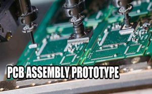
Prototype PCB Assembly Services at Kingda
Kingda provides Prototype PCB Assembly solutions for electronic product development and engineering validation.
Prototype projects can involve SMT, THT, or mixed-technology assembly depending on the PCB design and component requirements. The manufacturing process can include component preparation, solder paste printing, component placement, reflow soldering, through-hole assembly, inspection, and electrical testing as required.
For complex products, prototype manufacturing should be treated as an engineering validation stage rather than simply a small production run. Kingda can work with customers to evaluate manufacturability, assembly requirements, inspection needs, and testing considerations before a design progresses toward larger-scale manufacturing.
This approach can help engineering teams identify problems earlier, reduce unnecessary redesign cycles, and improve the transition from prototype builds to production.
Conclusion
Prototype PCB Assembly is an essential stage in the development of many electronic products. By manufacturing and testing a limited number of assembled boards before mass production, engineers can identify design weaknesses, verify component selection, evaluate manufacturability, and improve product reliability.
A successful prototype process typically includes component selection, schematic verification, PCB layout, PCB Manufacturing, component assembly, soldering, inspection, and PCB Testing. Both SMT Assembly and THT Assembly can be used depending on the product requirements.
The most effective prototype strategy combines rapid iteration with disciplined engineering and quality control. Prototype results should not only determine whether the current design works, but also provide useful information for improving manufacturability, reliability, testing, and production efficiency.
With appropriate design review, process control, and inspection, Kingda can support prototype PCB projects from initial assembly through engineering validation and preparation for production.