Inverter PCB Design: PCB Design, PCB Manufacturing, EMI/EMC & Thermal Management Guide
In modern power electronics, converting DC power into AC power is a fundamental function in many electronic and energy systems. An inverter PCB must handle high currents, high switching frequencies, and significant thermal loads while maintaining stable power conversion and reliable operation.
Unlike conventional low-power circuit boards, inverter circuit boards require careful attention to PCB Design, grounding, high-current routing, gate-driver circuits, isolation, electromagnetic interference (EMI), electromagnetic compatibility (EMC), and thermal management. Poor layout decisions can increase switching losses, create excessive voltage overshoot, generate electromagnetic noise, and shorten component lifetime.
For applications such as solar power systems, electric vehicles (EVs), industrial motor drives, energy storage systems, and power supplies, a well-engineered PCB Manufacturing process is equally important. Material selection, copper thickness, layer stackup, dielectric spacing, thermal structures, and manufacturing tolerances all affect the final performance of the inverter.
This guide explains the major principles of inverter PCB design and manufacturing, including grounding, power routing, decoupling, gate-driver layout, signal conditioning, EMI/EMC control, isolation, and thermal management.
What Is an Inverter PCB?
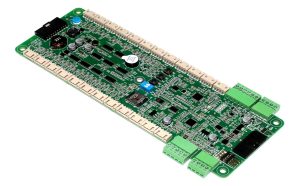
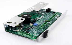
An inverter PCB is a printed circuit board designed to control and support the conversion of DC electrical power into AC power. Depending on the application, an inverter may use MOSFETs, IGBTs, SiC MOSFETs, or other power semiconductor devices as switching elements.
Inverter circuits are widely used in:
- Solar photovoltaic (PV) systems
- Energy storage systems
- Electric vehicles and charging systems
- Industrial motor drives
- Uninterruptible power supplies (UPS)
- Consumer appliances
- Industrial automation equipment
- Renewable energy systems
- High-power switching power supplies
A typical inverter system can include a power conversion stage, gate-driver circuits, a microcontroller or digital controller, current and voltage sensing circuits, auxiliary power supplies, communication interfaces, and protection circuits.
Because these functional blocks operate at different voltage, current, and switching levels, the PCB layout must carefully control current loops, return paths, parasitic inductance, and noise coupling.
A properly engineered Inverter PCB can improve power-conversion efficiency, reduce switching noise, simplify thermal management, and increase overall system reliability.
Key Inverter PCB Design Considerations
1. Grounding and Return-Path Design
Grounding is one of the most important aspects of inverter PCB design because high-current switching circuits can generate significant transient currents and voltage fluctuations.
A typical inverter may contain three major functional areas:
- Power conversion circuitry
- Control and microcontroller circuitry
- Inverter switching circuitry
Although these circuits may share a common system reference, they should not necessarily share unrestricted copper paths.
Sensitive control circuitry should be isolated from noisy high-current switching paths as much as practical.
Star Grounding
For some inverter architectures, star-grounding techniques can help prevent high-current switching currents from flowing through sensitive control-ground paths. The exact grounding strategy should be determined from the system topology, current paths, and switching behavior rather than applied as a universal rule.
Ground Planes
A properly designed ground plane provides a low-impedance return path and can help reduce electromagnetic radiation and noise coupling.
However, simply filling every unused PCB area with copper does not automatically improve performance. Ground pours should be connected appropriately and should not unintentionally create undesirable current loops.
Ground Bounce
Fast switching currents flowing through parasitic inductance can produce transient ground voltage differences, commonly referred to as ground bounce.
Excessive ground bounce can affect:
- Gate-driver signals
- Microcontroller inputs
- Current-sensing circuits
- Communication interfaces
- Protection circuits
Therefore, minimizing high di/dt loop inductance is essential in inverter PCB Design.
2. Power Pad and Power Component Layout
Power semiconductor packages often contain exposed pads or thermal pads that serve both electrical and thermal functions.
The PCB footprint must match the component manufacturer’s recommended land pattern and thermal requirements.
Thermal Pad Design
An exposed thermal pad may require multiple thermal vias to transfer heat into an internal or bottom copper plane. However, via size, pitch, number, and whether the vias are open or filled should be selected according to the package design and manufacturing capability.
High-Current Routing
High-current paths should generally use:
- Wider copper traces
- Copper pours or planes
- Short current paths
- Multiple vias when current must transition between layers
- Appropriate copper thickness
The objective is to reduce resistance, voltage drop, copper loss, and temperature rise.
For high-power inverter designs, trace width should not be selected solely from a generic width chart. Current level, copper thickness, allowable temperature rise, layer position, surrounding thermal environment, and manufacturing capability should all be considered.
3. Power Supply Design
The auxiliary power supply provides the required voltage rails for control ICs, gate drivers, sensors, communication circuits, and other low-voltage electronics.
A DC-DC converter or power-management IC (PMIC) may convert an input voltage into multiple output rails, such as:
- 5 V
- 3.3 V
- 1.8 V
- ADC reference or analog supply rails
The actual input and output voltage ranges depend on the selected IC and system architecture.
For example, an inverter controller may require a low-voltage supply for its microcontroller while a separate isolated or floating supply powers high-side gate drivers.
The power-supply layout should keep high-frequency switching loops compact and should separate noisy power nodes from sensitive analog and communication circuits.
4. Decoupling and Bypass Capacitors
Decoupling capacitors are essential for maintaining stable supply voltages and providing high-frequency current close to integrated circuits.
Decoupling Capacitor Placement
A decoupling capacitor should generally be positioned as close as practical to the IC power and ground connections.
The connection between the capacitor, power pin, and ground return should be short and low impedance.
For high-speed gate-driver circuits, even small parasitic inductances can contribute to voltage overshoot and ringing.
Bypass Capacitors
Bypass capacitors should be placed close to the VCC and GND or equivalent supply pins of the relevant device.
A well-designed multilayer stackup can also help reduce power-distribution impedance by placing power and reference planes appropriately.
Different capacitor values may be combined to address different frequency ranges, but the final selection should be based on the IC datasheet, switching frequency, transient requirements, capacitor characteristics, and measured behavior.
5. Gate-Driver Layout
The gate-driver section is one of the most sensitive areas of an inverter PCB.
The gate driver controls the switching behavior of MOSFETs, IGBTs, SiC devices, or other switching components. Poor gate-driver routing can cause excessive ringing, overshoot, switching losses, or even device failure.
Bootstrap Capacitor Placement
For a bootstrap-based high-side gate driver, the bootstrap capacitor should be positioned very close to the relevant driver pins.
The bootstrap diode, when used, should also be located close to the driver and connected with a short, low-inductance path.
Gate Resistors and Pull-Down Resistors
Gate resistors influence switching speed and can be used to control the trade-off between switching losses and electromagnetic noise.
Pull-down resistors should generally be located close to the corresponding gate and source/emitter reference so that the switching device remains in a defined state when the driver is inactive.
Minimize Gate-Drive Loop Area
The gate-drive signal and its return path should be routed close together to minimize loop area and parasitic inductance.
This is particularly important for high-speed SiC and other fast-switching power devices.
A compact gate-drive loop can help reduce:
- Voltage overshoot
- Ringing
- EMI
- Switching instability
- Unwanted gate voltage transients
Dead Time
Dead time is the interval between turning off one switching device and turning on its complementary device.
If the dead time is too short, both devices may conduct simultaneously, creating shoot-through and potentially damaging the power stage.
If the dead time is too long, additional conduction losses may occur.
Therefore, dead-time settings should be determined based on the switching devices, driver propagation delay, operating conditions, and system requirements.
High-Voltage Clearance and Creepage
High-voltage sections require appropriate electrical spacing.
Clearance refers to the shortest distance through air between conductive features, while creepage refers to the shortest distance along the surface of the insulating material.
The required values depend on factors such as:
- Working voltage
- Pollution degree
- Material group
- Altitude
- Insulation type
- Applicable safety standard
- System architecture
Therefore, a fixed value such as 2 mm should not be treated as universally sufficient for every inverter.
Switching-Node Control
High dv/dt switching nodes can generate significant common-mode and differential-mode noise.
These nodes should be kept compact and away from sensitive analog traces, communication lines, and control circuitry whenever possible.
6. Signal Conditioning and Current Sensing
Signal-conditioning circuits receive feedback from sensors and convert it into signals that can be safely and accurately processed by the controller.
Typical feedback signals include:
- Phase current
- DC bus voltage
- Temperature
- Motor position
- Battery voltage
- Motor speed
Current-sensing circuits require particularly careful PCB layout.
For low-side current sensing, the shunt resistor and sensing traces should be arranged to minimize the influence of high-current copper voltage drops.
Kelvin connections can be used where appropriate to separate the high-current path from the low-level measurement path.
Differential Routing
Current-sense signals should generally be routed as a matched differential pair when the sensing architecture supports it.
Filtering components should be positioned close to the measurement input, and the filter network should be designed according to the sensor bandwidth and control-loop requirements.
The objective is to prevent switching noise from being interpreted as a real current or voltage signal.
Important Inverter PCB Design Considerations
7. Isolated Secondary-Side Power Supply
Many inverter systems require isolated or floating power supplies for gate drivers, especially when the switching devices operate at different potentials.
The auxiliary power supply must provide the correct voltage, current, isolation, and transient performance required by the gate driver.
Bypass capacitors should be positioned close to the driver power pins to reduce supply impedance and minimize high-frequency voltage fluctuations.
The turn-on and turn-off current paths should be kept compact to reduce parasitic inductance.
In isolated gate-drive systems, the isolation barrier must also comply with the applicable safety requirements for the operating voltage and application environment.
8. EMI and EMC Considerations
EMI and EMC should be considered during the initial PCB Design stage rather than after the prototype has already failed compliance testing.
A high-power inverter can generate substantial electromagnetic noise because of rapid switching transitions and high di/dt and dv/dt values.
Important EMI/EMC considerations include:
- Switching-node area
- Gate-drive loop area
- DC-link capacitor placement
- Grounding strategy
- Cable routing
- Connector placement
- Common-mode current paths
- Differential-mode current paths
- Switching frequency
- Gate resistance
- Dead time
- Shielding
- Creepage and clearance
Reduce High-Frequency Loop Area
One of the most effective layout strategies is to minimize the area of high-frequency current loops.
For example, the DC-link capacitor should be placed as close as practical to the switching power stage so that the high-current commutation loop remains compact.
Avoid Unnecessary 90-Degree Routing
At high-speed and high-frequency nodes, designers often prefer 45-degree routing or smooth curves where appropriate.
However, the key objective is not simply eliminating every 90-degree corner. More important considerations include controlled impedance, current return paths, manufacturability, and minimizing unnecessary discontinuities.
Reduce Antenna Effects
Large copper loops and long cables can behave like unintended antennas.
Reducing loop area, improving return paths, and controlling cable and connector geometry can help reduce radiated emissions.
Common-Mode and Differential-Mode Noise
Differential-mode noise is associated with voltage and current differences between conductors, while common-mode noise occurs when unwanted signals appear relative to a common reference.
Both types should be considered when designing filters, grounding structures, shielding, and PCB layouts.
9. Isolation Between Control and Power Switching Sections
In many inverter architectures, the microcontroller, gate drivers, auxiliary power supplies, and high-power switching stage must be carefully separated.
The power switching section can generate significant electromagnetic noise and fast voltage transients. If sensitive control circuitry is routed too close to this area, noise may couple into the control system.
A practical PCB architecture may therefore divide the board into functional zones:
Control Section → Gate-Driver Section → Power Switching Section
This zoning approach helps control noise propagation and simplifies thermal and electrical analysis.
Connector and Cable Considerations
Gate signals and power signals may travel through connectors or cables.
Connector spacing, cable construction, cable length, and return-path design can influence parasitic inductance and electromagnetic coupling.
For high-speed gate-drive signals, the signal and return path should be designed as a controlled loop rather than treating the signal conductor independently.
10. Thermal Management
Thermal management is critical for inverter PCB reliability.
Power MOSFETs, IGBTs, SiC devices, rectifiers, inductors, transformers, and other power components can generate significant heat during operation.
Excessive junction temperature can reduce efficiency, accelerate component aging, and eventually cause thermal failure.
PCB Material Selection
Depending on power density and application requirements, designers may consider materials such as:
- FR-4
- Metal-core PCB materials
- Ceramic substrates
- High-performance laminate systems
- Specialized low-loss materials for RF-related functions
Material selection should consider thermal conductivity, dielectric performance, coefficient of thermal expansion (CTE), operating temperature, mechanical requirements, voltage isolation, and manufacturing capability.
FR-4 remains widely used for many inverter control and power boards, while ceramic or metal-core solutions may be advantageous in applications with demanding thermal requirements.
Thermal Vias
Thermal vias can transfer heat from a component pad into internal or bottom copper structures.
They are especially useful for power packages with exposed thermal pads.
The number and arrangement of thermal vias should be optimized to balance thermal performance, electrical performance, soldering requirements, and manufacturing constraints.
Copper Thickness
Increasing copper thickness can improve current-carrying capability and thermal spreading.
However, thicker copper also affects:
- Etching
- Plating
- Trace geometry
- Via design
- Minimum feature size
- Manufacturing cost
Therefore, copper thickness should be selected during the design-for-manufacturing stage rather than simply increased without considering the complete fabrication process.
11. Inverter PCB Stackup Design
A suitable multilayer stackup can significantly improve the electrical and thermal performance of an inverter PCB.
A typical stackup may include dedicated layers for:
- High-current power distribution
- Ground/reference
- Control signals
- Gate-drive signals
- Analog sensing
- Power planes
The exact layer arrangement depends on the power level, switching frequency, isolation requirements, mechanical dimensions, and manufacturing capabilities.
A properly designed stackup can help:
- Reduce loop inductance
- Improve return-current paths
- Reduce EMI
- Improve signal integrity
- Improve thermal spreading
- Simplify high-current routing
Stackup design should therefore be considered early in the PCB Manufacturing planning process.
12. Design for Manufacturing and Testing
A high-performance inverter PCB is not complete when the schematic and layout are finished.
The design must also be manufacturable, inspectable, testable, and repairable.
Important DFM and DFT considerations include:
- Appropriate trace and spacing rules
- Manufacturable via structures
- Adequate solder-mask clearance
- Component accessibility
- Test-point placement
- Thermal-pad design
- Copper balancing
- Controlled impedance where required
- Appropriate creepage and clearance
- Assembly tolerances
- Electrical test requirements
During PCB Manufacturing, inspection and testing may include AOI, electrical testing, X-ray inspection for selected assemblies, dimensional inspection, and functional testing depending on the product.
For high-reliability inverter systems, prototype validation should include measurements of switching waveforms, gate voltage, current, temperature, overshoot, ringing, and EMI behavior under representative operating conditions.
Common Inverter PCB Design Mistakes
Several PCB layout mistakes can significantly affect inverter performance.
1. Excessively Long High-Current Paths
Long power paths increase resistance and parasitic inductance, resulting in additional losses and voltage transients.
2. Poor Gate-Driver Placement
Placing the gate driver too far from the switching device increases gate-loop inductance and can cause ringing.
3. Improper Decoupling
A capacitor with the correct nominal value may still perform poorly if it is connected through long, high-inductance traces.
4. Mixing Sensitive and Noisy Circuits
Analog sensing and communication circuits should not share uncontrolled return paths with high-current switching circuits.
5. Insufficient Thermal Design
Ignoring junction temperature and heat-transfer paths can lead to thermal runaway, reduced efficiency, and premature component failure.
6. Inadequate Electrical Spacing
Creepage and clearance must be calculated according to the applicable safety requirements rather than relying on a universal spacing value.
7. Ignoring Manufacturing Constraints
A theoretically excellent layout may become expensive or impossible to manufacture if it requires unrealistic trace widths, spacing, via structures, copper thickness, or tolerances.
Inverter PCB Design and Manufacturing with Kingda
For demanding inverter applications, the PCB supplier should be involved early in the development process rather than only after the design has been completed.
Kingda provides PCB fabrication and PCBA capabilities covering prototype development and production applications.
For inverter-related projects, a manufacturing partner can contribute to:
- PCB stackup selection
- High-current PCB design review
- DFM analysis
- Copper-thickness evaluation
- Thermal design considerations
- PCB fabrication
- SMT assembly
- Through-hole assembly
- AOI and X-ray inspection
- Electrical testing
- Functional testing
- Final assembly and integration
Early collaboration between the engineering and manufacturing teams can help identify problems related to trace width, copper distribution, thermal structures, component placement, clearance, manufacturability, and assembly before production begins.
This approach can reduce redesigns and improve the transition from prototype to volume PCB Manufacturing.
How to Improve Inverter PCB Reliability
A reliable inverter PCB requires coordination between electrical, mechanical, thermal, and manufacturing considerations.
A practical development process includes:
- Define voltage, current, switching frequency, and power requirements.
- Select appropriate power semiconductor devices.
- Define the PCB stackup and copper structure.
- Separate power, gate-driver, analog, and control areas.
- Minimize high-current and high-frequency loop areas.
- Optimize gate-driver placement and routing.
- Position decoupling and bootstrap capacitors close to their associated devices.
- Design appropriate grounding and return paths.
- Calculate creepage and clearance according to applicable standards.
- Analyze thermal performance.
- Perform DFM and DFT reviews.
- Prototype and validate electrical performance.
- Measure switching waveforms, ringing, temperature, and EMI.
- Correct layout or component issues before mass production.
- Establish controlled PCB Manufacturing and assembly processes.
This systematic approach is more reliable than attempting to solve EMI, thermal, or switching problems only after the first prototype has been built.
Conclusion
Inverter PCB design is considerably more demanding than conventional low-power PCB design because the board must simultaneously manage high current, high voltage, fast switching, thermal stress, electromagnetic noise, and sensitive control signals.
The most important considerations include grounding, high-current routing, power-pad design, decoupling, gate-driver layout, current sensing, electrical isolation, EMI/EMC control, thermal management, stackup design, and manufacturability.
A successful PCB Design must not only deliver the required electrical performance but also be practical for PCB Manufacturing, assembly, inspection, testing, and long-term operation.
For high-power applications such as EV motor drives, solar inverters, industrial equipment, and energy-storage systems, early collaboration between the design team and manufacturing partner can significantly reduce development risk and improve product reliability.
Article Summary
An inverter PCB is the electrical and mechanical foundation of many modern DC-to-AC power conversion systems. Because inverter circuits involve high current and fast switching, the PCB layout must carefully control grounding, current loops, gate-drive signals, parasitic inductance, EMI/EMC, creepage and clearance, and thermal performance.
Good PCB Design practices should be combined with appropriate materials, copper thickness, stackup structures, DFM analysis, assembly processes, and electrical testing. By integrating design, simulation, manufacturing, inspection, and validation from the beginning, engineers can develop inverter PCBs with better efficiency, lower electromagnetic noise, improved thermal performance, and greater long-term reliability.