High Precision RF PCB Manufacturing From 5G-A to 6G
Telecom investment plans rarely name circuit boards, yet the numbers behind them decide which factories stay busy. A spending programme covering information infrastructure through 2030 puts high precision RF PCB manufacturing at the centre of the next upgrade cycle, alongside compute capacity and new terminal devices.
Radio units, switching equipment and servers each place a different demand on the board. Frequency determines how much the dielectric matters, layer count determines how much the lamination process matters, and physical size determines how much impedance consistency matters across a single panel. A factory prepared for one of those is not automatically prepared for the others.
Where the Investment Actually Lands
Coverage expansion mostly consumes conventional boards, and that demand is well understood by every supplier. The part of the programme that changes manufacturing requirements is the combination of higher frequency radio, denser compute and smaller terminals, because each of those raises a different process limit.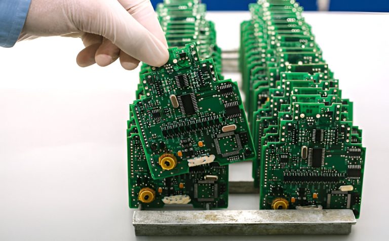
Buyers should read such plans as a change in product mix rather than as a general increase in volume. The factories that benefit are the ones already running materials and tolerances that ordinary capacity cannot reach.
Why Frequency Raises the Manufacturing Bar
As operating frequency rises, the electrical result depends more on geometry and material than on the schematic. Conductor width variation that was harmless at lower frequencies becomes a measurable insertion loss difference, and a small change in dielectric constant shifts phase across the band.
The shift moves requirements into the factory. Etch tolerance, layer thickness control and impedance uniformity have to hold across the whole panel, not only at the coupon. For telecommunications PCB programmes, that turns the fabrication partner into part of the design team rather than a supplier working from a Gerber file.
Dielectric Stability and Copper Roughness
Two material properties dominate performance at high frequency: how stable the dielectric constant is over temperature and frequency, and how rough the copper surface is where it meets the laminate. Roughness increases conductor loss because current crowds into the peaks of the profile.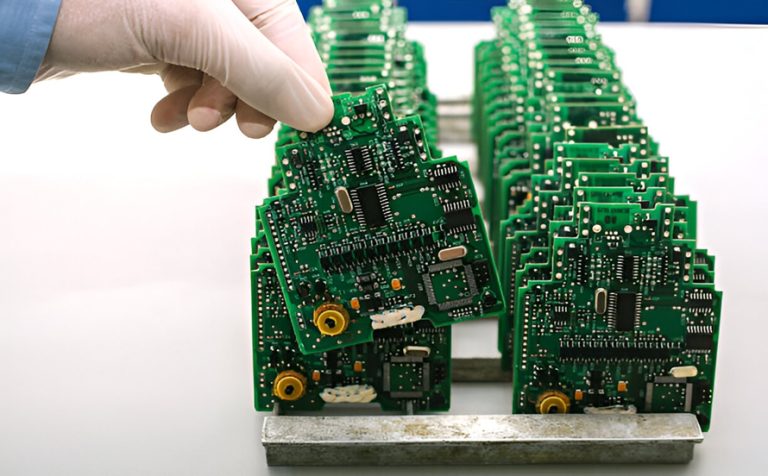
Both properties are set by the material supplier, which limits what a fabricator can change. What the fabricator controls is how consistently the material is processed, and whether the lamination cycle preserves the properties the designer selected.
Etch Tolerance and Impedance Consistency
Controlled impedance is not a single measurement. It is a distribution across every trace on every panel, and the width of that distribution decides whether a radio unit performs consistently in production or only in the laboratory. Etching is where most of that distribution is created.
Fine line capability without uniformity is not useful for RF work. Designers should ask how impedance is measured, at what frequency, on how many coupons per panel, and what the acceptance window is. A factory that answers those questions with data is one that has the process genuinely under control.
AI Compute Pushes a Different Limit
Compute hardware raises complexity rather than frequency alone. Accelerators and switch chips demand many high speed differential pairs, which drives layer counts upward and forces more lamination cycles, tighter registration and deeper drilling. Each added layer multiplies the number of opportunities for a stack to drift.
That is why AI compute hardware has become a test of high layer count capability rather than of raw capacity. The limiting factor in most programmes is not how many panels a factory can press but how many it can press without losing registration.
Back Drilling and Residual Stubs
At high data rates a via stub behaves like a small antenna, reflecting energy back into the channel. Back drilling removes most of the unused barrel, but the process demands depth control measured in fractions of a millimetre across a panel that may be several millimetres thick.
Drill depth variation is the failure mode. Tool wear, panel thickness tolerance and machine stability must all be monitored, and the fabricator should be able to show measurement data rather than a nominal specification, because the difference shows up as jitter in a link that otherwise tests perfectly.
Three Demand Paths, One Manufacturing Problem
Radio equipment wants low loss materials and precise impedance. Data centre equipment wants high layer counts, back drilling and dense routing. Smart glasses and similar wearables want thin boards, fine lines and flexible or rigid flex constructions. The products look unrelated, but the underlying capability overlaps.
The overlap is precision. All three paths require a factory that can hold tight tolerances on difficult materials, and the HDI and rigid flex capability required for terminals is the same discipline that supports dense compute boards. That is why investment in one area often pulls the other two forward.
Smart Glasses Compress the Board Instead
A wearable has no room for a conventional stack. A camera, a wireless radio, a processor, power management and sensors have to share a curved frame, often with the battery occupying the most generous volume. The result is a small board with fine geometry, blind vias and frequent flex sections.
Manufacturing such a board stresses different things: thin material handling, microvia reliability and assembly tolerance. Suppliers who only know large multilayer panels find wearables difficult, while specialists in dense small boards often find RF work unfamiliar. Few factories cover both without effort.
Qualifying a Process Before the Standard Exists
Next generation radio standards are still being written while the hardware is being prototyped. Designs therefore change quickly, and the factory has to qualify materials and processes for products whose final specification is not yet fixed. That calls for flexible process development rather than optimised mass production.
Practical preparation includes building a library of material data measured in production rather than copied from datasheets, and keeping a test vehicle that can be run quickly when a new laminate appears. Suppliers who can do that help customers move early without committing to a specification that may change.
What Telecom Buyers Should Verify
Buyers in this sector should look for evidence rather than promises. Which high frequency materials are actually processed, on what equipment, with what documented controls? Which measurements are taken on production panels? How is a drift in impedance detected before shipment rather than after installation?
Process control also has to be visible in the paperwork. A partner able to present process control and traceability data alongside the boards is describing a manufacturing system, and that is what a multi-year infrastructure programme needs from its supply chain.
Small Boards, Tight Assembly Windows
Wearable and terminal products stress assembly as much as fabrication. Fine pitch components on a thin board leave little room for placement error, and flexible sections complicate handling further. The reflow profile has to suit a board that behaves very differently from a rigid panel of the same thickness.
This is why terminal programmes benefit from a partner who builds prototype assemblies as well as prototype boards. Learning about flexible circuit assembly behaviour early prevents a design from being frozen around a fabrication capability that later proves awkward to populate at volume.
Layer Count Discipline in Compute Designs
More layers solve routing problems, but they also add lamination cycles, cost and opportunities for registration error. Designers working on AI compute hardware should decide early how many layers are genuinely required and how many are simply convenient.
The saving is not only material. A stack with fewer layers presses faster, drills faster and yields more, which matters when a programme needs thousands of panels rather than a handful of prototypes. Layer count discipline is one of the few levers that improves both cost and delivery.
Material Lead Time as a Design Input
High frequency laminates are made by a small supplier base, and their delivery times move with demand from data centre and automotive programmes. A design released against a grade with a twelve week lead time starts its production phase already behind schedule.
Telecommunications PCB programmes are therefore well served by confirming availability before layout rather than after. A qualified alternative material, validated in production and not only on a datasheet, keeps a project moving when the preferred grade tightens.
Testing Radio Boards Properly
A radio board can pass continuity testing and still fail in service. Meaningful verification includes insertion loss measurement, impedance checks on production coupons and functional testing at the frequencies the product will actually use. Test fixtures belong to the design phase rather than to the production phase.
Keeping fabrication close to board level test also shortens the investigation when a panel misses its loss budget. The drill records and the measurement data sit in the same system, so the cause can be found in hours instead of days.
Where Precision Becomes the Bottleneck
As the upgrade progresses, the scarce resource will not be any single material. Semiconductor-like precision in lamination, drilling and plating will set the ceiling on what the industry can deploy, and the factories that reach that standard first will define the schedule for everyone else.
That is why manufacturing process deserves as much attention as the investment figure itself. Capacity can be added quickly, but precision has to be built deliberately, one process step at a time, and it cannot be bought late in a project without risking the delivery date.