Optical Module PCB: mSAP, 800G and the High Speed Shift
Optical interconnect used to sit at the edge of the data centre discussion. It now sits at the centre of it, because adding accelerators without adding bandwidth simply moves the bottleneck. That shift has turned the optical module PCB into one of the most demanding products in volume production today.
Revenue reported by major board makers from 800G class optical products grew by an order of magnitude in a single quarter, which is a signal about interconnection rather than about any one company. When optical links scale that quickly, the boards inside them change specification just as quickly.
Where the Growth Is Coming From
Every accelerator added to a cluster needs a path to memory, to storage and to other accelerators. Switch capacity and optical links therefore expand alongside compute, and they expand with increasingly aggressive electrical requirements because the distance and the data rate both keep rising.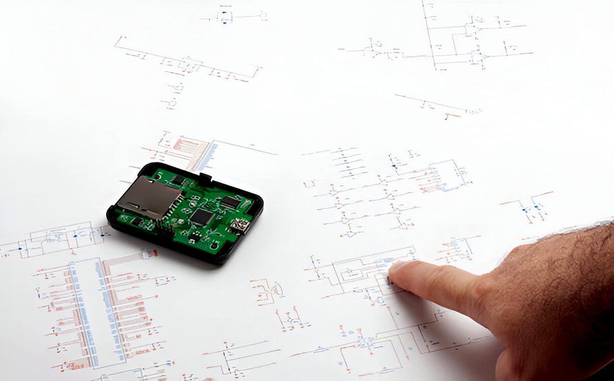
The boards that support this are not ordinary multilayer products. They combine high layer counts, dense differential routing, controlled impedance and strict loss budgets, which places them among the few product families where process capability, rather than price, decides who can supply them. The demand is structural rather than cyclical, and it will not reverse while cluster sizes continue to grow.
From 800G to 1.6T
Module speeds double roughly every generation, and each doubling reduces the electrical margin available to the board. Loss that was tolerable at 400G becomes a design problem at 800G and a hard limit at 1.6T, even though the physical dimensions of the module barely change.
Engineers respond with materials, with via structures and with routing discipline, but there is a limit to how much can be recovered passively. At some point the trace geometry itself has to become finer, which pushes mainstream production toward advanced line formation techniques.
Why Fine Lines Matter More Than Ever
More channels in the same board area means narrower conductors and tighter spacing. Conventional subtractive etching struggles at these dimensions, because the etchant attacks the sides of a trace as well as its top, leaving a trapezoidal cross section that changes impedance and increases loss.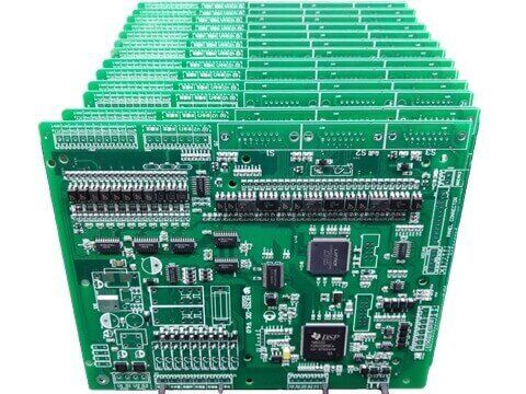
Fine line capability is therefore not a marketing feature. It determines how many high speed channels fit on a module board and how consistently each of those channels performs, which decides whether the module meets its specification across a production lot rather than in a sample.
What mSAP Changes on the Factory Floor
Modified semi additive processing reverses the usual logic. Instead of etching away unwanted copper, the process starts with a very thin seed layer and builds up the conductors by plating into a pattern defined by photoresist. The result is a rectangular trace with a more predictable cross section.
The sequence adds steps and demands tighter control over surface preparation, plating uniformity and resist adhesion. That is why board fabrication at the fine line end of the market looks more like semiconductor processing than like traditional circuit board work.
High Layer Counts and the Pressing Cycle
Switch boards and backplanes continue to grow in layer count because the number of high speed lanes grows. Each lamination cycle adds registration risk, and registration is the parameter that limits how thin a dielectric can be before the impedance window becomes unmanageable.
Layer count also multiplies cost, because material and processing are consumed at every stage. A factory that can press a dense stack without losing alignment is therefore more valuable than one with simply more press capacity, even though the second is easier to measure.
Back Drilling and the Stub Problem
A via that passes through more layers than it needs leaves a stub behind, and at these data rates a stub acts as a resonant element that reflects energy back into the channel. Back drilling removes the unused portion, but it demands depth control measured in fractions of a millimetre.
The failure mode is subtle. A stub that is slightly too long may still pass a continuity test while degrading the eye diagram enough to reduce link margin. Progressive production process control on drill depth is the only reliable protection against that outcome.
Impedance Windows Tighten to Five Percent
Differential impedance targets that once allowed a ten percent window now often specify five percent, because the loss budget cannot accommodate a wider spread. That narrows the acceptable range of line width, dielectric thickness and copper thickness simultaneously.
Meeting it requires measurement, not assumption. Coupon design, measurement frequency, and the number of coupons per panel all matter, and the data has to be used to correct the process during the run rather than merely recorded for the customer file.
Low Loss Material and Copper Roughness
At high frequency, conductor loss depends partly on how rough the copper surface is where it meets the laminate. Rougher foil means a longer effective current path and more loss, so smooth foil grades have become standard in high speed designs.
That creates a manufacturing tension. Smooth foil adheres less readily to the resin, so lamination parameters and surface treatment have to be adjusted to protect peel strength without sacrificing the electrical benefit the material was chosen for.
Capital Intensity Reshapes the Supply Chain
Building capability for these products requires laser drilling, vacuum pressing, high precision exposure, advanced plating and automated inspection, and the investment is measured in hundreds of millions rather than millions. Barriers to entry rise accordingly.
The consequence is a supply chain with fewer participants at the top end and more room for specialists below it. High volume manufacture and high volume assembly cannot serve every engineering need, and much of the innovation in this market still happens in smaller, more responsive batches.
Two Boards in One Link
An optical link involves at least two quite different boards. The module itself is a compact, fine line product concerned with loss and impedance, while the switch or line card is a large, layer intensive board concerned with routing density and power delivery.
Both must meet the same electrical standard even though they are built with different processes and inspected with different methods. A supplier able to produce both, and to hold a single quality system across them, removes a coordination burden from the customer.
The Same Pattern in Automotive and Robotics
Centralised vehicle computing puts cameras, radar and vehicle networks onto a small number of high speed platforms, so automotive boards are beginning to look like data centre boards. Robotics adds flexible interconnect and heavy copper power sections alongside the same high speed routing.
The result is that capability developed for one industry transfers quickly to others. Fine line etching, controlled impedance and low loss materials are no longer niche skills; they are shared requirements across several growing markets at once.
Why Small Batch Capability Still Matters
Major investment goes into volume capacity, but most new products are validated in small quantities first. Engineering builds, early customer samples and qualification lots all require the same processes as production, just at a fraction of the volume.
A supply chain that can only serve volume pushes those early builds into a gap. Factories that combine prototype support with genuine high end capability let customers qualify a process before committing to a production order, which reduces risk for both sides.
Prototype Windows in a Fast Moving Market
Design cycles in optical and AI hardware are short. A layout may change twice before the first qualification lot, and each change can alter stack up, impedance targets and drill strategy. Turnaround time on those revisions affects the product schedule directly.
This is where advanced PCB capability and engineering responsiveness interact. A factory that can review a stack up in days and fabricate a revision in a week is more useful to a development team than one with greater capacity but a slower feedback loop.
Quality Loops That Catch Drift Early
High speed products fail quietly. A drift in etch factor or plating thickness may not create a visible defect, but it changes impedance and loss in ways that only appear in measurement. Catching that drift requires measurement embedded in the production routine.
Useful process control links coupon results back to the panels they came from, so a customer question can be answered with data rather than a recalled impression. In this market, that traceability is often the difference between a sustained programme and a single order.
What Buyers Should Verify Now
Ask which fine line process is used and what the smallest reliable line and space is in production rather than in a demonstration. Ask how differential impedance is measured, how often, and what the observed distribution looks like across a normal production week.
Then ask how the supplier handles a stack up change, a material shortage and a yield excursion. Optical programmes run for years, and the answers to those three questions will matter far more than the price on the first purchase order, which is likely to be the smallest order placed during the life of the programme.