In high-speed PCB design, the ground via array beneath a BGA package is easy to overlook. Engineers may confirm that a continuous ground plane exists and assume that the return-current path is therefore sufficiently low impedance.
At high frequencies, however, a continuous ground plane alone does not guarantee an effective return path at the package level.
A recent high-speed FPGA design illustrates the problem. During board-level testing, a 40 Gbps SerDes channel showed significant eye-diagram degradation, while measured power-rail ripple was substantially higher than the target. At the same time, an adjacent LVDS interface showed a sudden increase in bit errors.
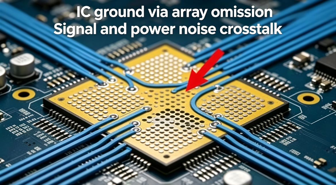
Cross-section analysis revealed that the ground via array beneath the BGA had insufficient local coverage around the power and signal transition areas. The issue was not the complete absence of a ground plane. Instead, the local ground return path was too far away from the corresponding power and signal structures.
This distinction is critical in high-speed BGA PCB design.
The purpose of a ground via array is not simply to provide electrical continuity to ground. It is also to provide a short, low-inductance path for high-frequency return current and to help control electromagnetic coupling between power and signal structures.
1. Why Ground Via Placement Matters at High Frequencies
At low frequencies, engineers can often focus on DC resistance and overall ground-plane continuity.
At high frequencies, inductance becomes increasingly important.
When a signal transitions between layers or enters and exits a BGA package, its return current needs a nearby path. If an appropriate ground via is not available close to the signal transition, the return current must spread through a longer path before reaching the nearest low-impedance ground connection.
That additional path introduces parasitic inductance.
The basic relationship is:
Xₗ = 2πfL
where:
- Xₗ is inductive reactance
- f is frequency
- L is inductance
As frequency increases, even a relatively small amount of parasitic inductance can produce a meaningful impedance.
This is why a ground via that is electrically “connected” but physically far from the signal transition may not provide the same high-frequency performance as a nearby via.
Local Return Path vs. Global Ground Plane
A large ground plane provides the overall reference structure for the PCB. However, the high-frequency return current associated with a BGA transition tends to follow the path of lowest impedance.
Therefore, the engineering question is not simply:
“Is there a ground plane?”
It is:
“Is there a sufficiently short and low-inductance ground return path at the transition?”
This is particularly important for PCIe, SerDes, high-speed Ethernet, LVDS, DDR, and other interfaces with fast edge rates.
2. How Insufficient Ground Via Coverage Can Increase Noise
An inadequate via array can affect both signal integrity and power integrity.
When high-frequency return current cannot find a nearby ground via, it may spread into adjacent structures or travel around the BGA region.
This can increase:
- Return-path inductance
- Local voltage fluctuations
- Ground bounce
- Electromagnetic coupling
- Common-mode conversion
- Crosstalk
- Power-distribution-network impedance
The result can appear in different forms depending on the system architecture.
For a high-speed differential channel, the effect may include increased mode conversion, additional insertion loss, or eye-diagram degradation.
For the power distribution network, insufficient local grounding and inadequate decoupling can contribute to higher transient voltage fluctuations.
For adjacent LVDS or other sensitive interfaces, unwanted coupling may increase the observed error rate.
This is why power integrity and signal integrity should not always be treated as completely independent problems.
3. Ground Via Density Should Follow Electrical Requirements
There is no single ground-via density that is universally correct for every BGA package.
The required density depends on:
- Signal edge rate
- Operating frequency
- BGA pitch
- Package escape structure
- PCB layer stackup
- Dielectric thickness
- Ground-plane structure
- Power distribution network
- Via diameter
- Via inductance
- Signal transition geometry
- Manufacturing capability
For high-speed designs, it is therefore more useful to establish a design rule based on the electrical transition and return-current path rather than simply specifying a fixed number of vias per square millimeter.
High-Speed Interfaces
For interfaces operating at very high data rates, such as 25 Gbps and above, designers should prioritize dense and locally distributed ground connections around critical transition areas.
The ground vias should be positioned so that the return current does not have to travel unnecessarily long distances before reaching the reference structure.
For BGA escape routing, ground vias can also be used strategically between or around sensitive signal transitions to reduce coupling.
Medium-Speed Interfaces
For interfaces in the intermediate speed range, the same principle applies, but the required via density may be less aggressive.
Designers should evaluate the complete stackup and signal edge rate rather than using data rate alone as the design criterion.
Two interfaces with the same nominal data rate can have different return-current behavior because their package, driver, rise time, routing geometry, and layer transitions are different.
Lower-Speed Applications
For lower-speed circuits, a less dense ground-via structure may be sufficient.
However, ground-via placement still matters for power distribution, EMI control, thermal design, and sensitive analog circuits.
The objective should always be to maintain an appropriate return path rather than maximize the number of vias without considering their actual electrical function.
4. Two-Dimensional Verification: Coverage and Offset
A practical way to review a BGA ground return path is to evaluate two dimensions:
1. Horizontal coverage
Determine whether ground vias are sufficiently distributed around the relevant BGA power, ground, and signal transition regions.
2. Vertical alignment
Check the distance between the BGA pad, PCB via structure, reference plane, and the corresponding power or ground connection through the stackup.
These two checks should be performed using actual manufacturing layers rather than relying only on the top-layer silkscreen.
Use CAM Data for Verification
During the layout review, engineers can overlay:
- BGA pad layer
- Via layer
- Power-plane layer
- Ground-plane layer
- Solder mask
- Drill layer
- Copper layers
CAM analysis can then be used to identify areas where the ground-via structure is unexpectedly far from critical power or signal transitions.
For production designs, this type of review is more reliable than judging via locations from the component outline alone.
5. Do Not Treat Every Ground Via as Electrically Equivalent
One common mistake is to count every via connected to ground as an effective high-frequency ground via.
In reality, the electrical effectiveness of a via depends on its complete structure.
Important factors include:
- Via barrel length
- Via diameter
- Pad size
- Antipad geometry
- Stub length
- Connection to reference planes
- Nearby copper structures
- Distance from the signal transition
- Number of parallel ground vias
Via Stubs Can Matter
A long via stub can introduce an additional discontinuity at high frequencies.
For demanding high-speed interfaces, designers should evaluate whether unnecessary stubs remain after layer transitions.
Back-drilling, blind vias, microvias, or other optimized via structures may be considered when the signal-speed and channel-length requirements justify them.
The correct solution depends on the stackup and fabrication capability.
6. Why a Ground Plane Cannot Always Replace a Local Via Array
Another common assumption is that a large internal ground plane automatically compensates for insufficient local ground vias.
It does not.
A reference plane provides a low-impedance distributed conductor, but the connection from the BGA structure to that plane still depends on the via and pad geometry.
If the signal transition is physically separated from the nearest ground connection, the current must still travel through a longer path before reaching the plane.
At high frequencies, this additional path can introduce enough inductive impedance to affect signal and power behavior.
Therefore, BGA ground vias should be considered part of the complete transition structure rather than merely connections to an otherwise ideal ground plane.
7. Consider the Power-Integrity Network Together With Ground Vias
The relationship between ground vias and power noise is especially important around FPGA, ASIC, CPU, and high-speed transceiver packages.
High-speed devices can generate rapid current transients.
The local power-distribution network must provide a low-impedance current path from the power source to the device and back through the corresponding return network.
A practical design review should therefore consider:
- Power vias
- Ground vias
- Decoupling capacitors
- Capacitor placement
- Plane capacitance
- Power-plane geometry
- Ground-plane geometry
- Via inductance
- Package parasitics
A decoupling capacitor located several millimeters away from the package may have a very different high-frequency effect from one connected through a short, low-inductance via structure directly adjacent to the power and ground pads.
This is why simply increasing the total capacitance does not always solve high-frequency power noise.
8. Three Common BGA Ground-Via Design Mistakes
Mistake 1: Counting Via Quantity Without Checking Location
A design may contain a large number of ground vias but still have poor high-frequency performance if those vias are concentrated far away from the critical BGA transitions.
Via quantity is not equivalent to via effectiveness.
The location and connection path must be evaluated together.
Mistake 2: Ignoring the Reference-Plane Transition
When a high-speed signal changes layers, the associated return current may also need to transition between reference structures.
If the reference plane changes from ground to power, or if a plane is interrupted by an antipad or routing channel, a nearby stitching capacitor or ground-via structure may be required to provide a controlled return path.
This is particularly important in multilayer high-speed PCB stackups.
Mistake 3: Placing Vias Without Considering Manufacturing Constraints
A very dense via structure may improve electrical performance but create manufacturing challenges.
Designers must consider:
- Minimum drill diameter
- Pad diameter
- Via-to-via spacing
- Via-to-pad clearance
- Aspect ratio
- Registration tolerance
- Solder mask clearance
- BGA pitch
- Via filling requirements
For HDI or microvia structures, the PCB manufacturer should be involved early in the design process.
9. Material and Stackup Effects Must Be Included
Ground-via requirements cannot be separated from the PCB stackup.
Important parameters include:
- Dielectric thickness
- Dk
- Df
- Copper thickness
- Copper roughness
- Plane spacing
- Board thickness
- Via geometry
A thinner dielectric between a signal layer and its reference plane can reduce the physical distance that the return field needs to cross and can affect coupling and impedance.
Similarly, low-loss or low-Dk laminates can change the electromagnetic behavior of the interconnect.
However, material changes should not automatically be interpreted as allowing a proportional reduction in ground-via density. The complete electromagnetic structure should be simulated or verified before changing established design rules.
10. A Practical Verification Workflow for High-Speed BGA Designs
For high-speed FPGA, ASIC, SerDes, and networking boards, Kingda recommends treating the BGA region as a dedicated SI/PI review area.
A practical workflow is:
Step 1 — Identify critical interfaces
Mark PCIe, SerDes, Ethernet, LVDS, DDR, clock, and other sensitive high-speed nets.
Step 2 — Map signal transitions
Identify every layer transition, via structure, BGA escape route, and reference-plane transition.
Step 3 — Map the return path
Verify that a nearby ground connection is available wherever the signal’s reference structure changes.
Step 4 — Review ground-via coverage
Check the distribution of ground vias around signal and power structures rather than simply counting the total number.
Step 5 — Check via geometry
Review diameter, pad, antipad, stub length, and connection to the reference planes.
Step 6 — Perform SI/PI simulation
For critical channels, compare impedance, insertion loss, crosstalk, mode conversion, and eye-diagram behavior.
Step 7 — Correlate With physical measurement
When prototypes are available, TDR, VNA, power-rail measurements, and eye-diagram testing can be used to correlate the simulation model with the physical board.
11. What to Do When the PCB Has Already Entered Production
If a prototype has already been fabricated and testing shows unexpected signal or power noise, the first step should be root-cause analysis rather than immediately adding vias.
Review:
- BGA via placement
- Ground-plane continuity
- Power-plane structure
- Decoupling network
- Reference-plane transitions
- Via stubs
- Differential-pair routing
- Stackup parameters
- Material models
- Package and connector models
Possible corrective actions include modifying the ground-via structure, adding stitching structures, optimizing decoupling placement, changing the layer transition strategy, or using HDI structures where appropriate.
For an already fabricated PCB, however, the available repair options are limited by component accessibility, board construction, manufacturing tolerances, and reliability requirements. Any laser-drilled or filled-via modification should therefore be treated as a controlled engineering change rather than a universal repair method.

12. Kingda’s Approach to BGA Ground Via Design
At Kingda, BGA ground-via design can be evaluated as part of the complete high-speed PCB manufacturing and signal-integrity workflow.
Rather than defining a ground-via requirement solely by package size or a fixed via-density number, the design can be reviewed according to:
- Interface speed and edge rate
- BGA pitch
- PCB stackup
- Dielectric thickness
- Ground-plane structure
- Power-distribution network
- Via geometry
- Reference-plane transitions
- Manufacturing capabilities
- SI/PI requirements
For demanding FPGA, ASIC, SerDes, networking, and high-speed backplane applications, this approach helps engineers identify whether the ground-via array actually provides the intended low-inductance return path.
The objective is not to maximize the number of vias. It is to place the right ground connections in the right locations while maintaining manufacturability and signal-integrity performance.
13. Conclusion
A BGA ground-via array is much more than a collection of connections to the ground plane.
For high-speed PCB designs, the position, geometry, and connection path of each relevant ground via can influence return-current inductance, power integrity, crosstalk, and signal integrity.
A board can have a continuous ground plane and still suffer from local return-path discontinuities if the ground vias are too far from critical BGA transitions.
The key design principle is therefore:
Do not evaluate ground vias by quantity alone. Evaluate the complete high-frequency return path.
For high-speed BGA PCB design, engineers should verify via coverage, reference-plane transitions, via geometry, stackup, power distribution, and SI/PI behavior together.
By combining careful BGA ground vias placement with structured SI/PI verification, engineers can reduce the risk of high-speed signal degradation and unwanted power noise coupling while maintaining a practical and manufacturable PCB design.