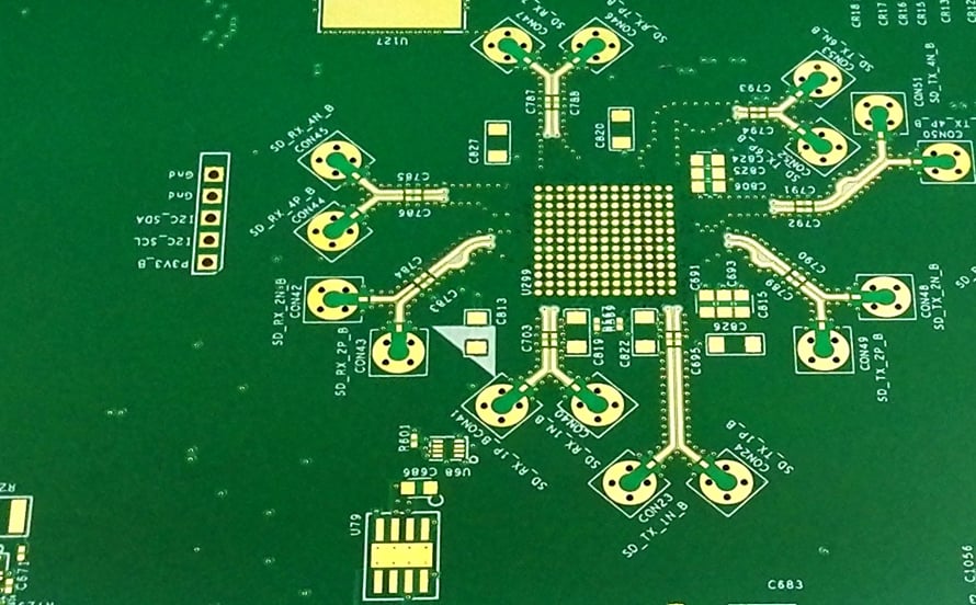
In high-speed multilayer PCB design, engineers often rely on the dielectric constant (Dk) provided in a laminate datasheet when calculating controlled impedance. The problem is that a Dk value measured at a low frequency cannot always accurately represent the electrical behavior of the same material at hundreds of megahertz or several gigahertz.
This difference is related to frequency dispersion, a material characteristic in which the effective dielectric properties change with signal frequency.
When a low-frequency Dk value is directly entered into a high-speed simulation, the calculated PCB impedance may differ from the impedance measured on the finished board. This issue can become important in DDR interfaces, high-speed Ethernet, PCIe, SerDes, RF circuits, and other multilayer designs where impedance tolerances are relatively tight.
Understanding the relationship between PCB dielectric constant, frequency, material structure, and transmission-line geometry is therefore essential for reliable impedance control.
What Is Frequency Dispersion in PCB Materials?
Frequency dispersion describes the change in a dielectric material’s electromagnetic response as frequency changes.
PCB laminates are not electrically ideal materials. Their dielectric behavior is influenced by factors such as:
- Resin chemistry
- Glass-fiber structure
- Resin content
- Frequency
- Temperature
- Moisture
- Measurement method
- Signal propagation mode
At different frequencies, polarization mechanisms inside the dielectric material respond differently to the applied electromagnetic field. As a result, the effective dielectric constant used for transmission-line calculations can vary with frequency.
For many conventional FR-4 materials, the reported Dk tends to change as frequency increases. However, the magnitude and direction of the change depend on the specific laminate and the measurement method.
Therefore, engineers should avoid assuming that one Dk value represents the material across the entire frequency spectrum.
Why Low-Frequency Dk Can Cause High-Speed Impedance Errors
A transmission line’s characteristic impedance depends on its geometry and the electromagnetic properties of the surrounding dielectric.
A simplified relationship can be expressed conceptually as:
[Z_0 \propto \frac{1}{\sqrt{Dk}}]
For a fixed transmission-line geometry, a higher effective Dk generally results in a lower characteristic impedance, while a lower effective Dk generally results in a higher impedance.
This explains a common simulation problem.
Suppose an engineer uses a Dk value measured at 1 MHz to design a transmission line operating with significant high-frequency content. If the effective Dk at the relevant frequency is lower than the value used in simulation, the actual impedance can be higher than the simulated result.
The difference may become large enough to exceed the project’s impedance tolerance.
However, the actual relationship is more complicated than simply replacing one datasheet Dk number with another. PCB transmission lines are affected by:
- Frequency-dependent Dk
- Glass-weave effects
- Copper roughness
- Trace geometry
- Resin content
- Layer construction
- Reference-plane spacing
- Differential coupling
This is why high-speed impedance design should use material data that is relevant to the actual stackup and operating frequency.
Dk and Df Must Be Considered Together
When evaluating a high-speed laminate, engineers should not focus exclusively on Dk.
The dielectric loss factor, commonly represented as Df, also changes with frequency and affects high-speed signal transmission.
Dk primarily influences propagation characteristics and impedance, while Df is associated with dielectric loss.
As signal frequency and transmission distance increase, dielectric loss can become a significant contributor to total insertion loss.
A high-speed channel therefore has two related but different requirements:
Impedance control → accurate transmission-line geometry and dielectric properties
Signal-loss control → appropriate dielectric loss characteristics and channel construction
A PCB can have an acceptable nominal impedance and still suffer from excessive insertion loss if its dielectric and copper-loss characteristics are unsuitable for the channel.
For this reason, Df should be reviewed together with Dk when selecting materials for demanding high-speed applications.
Different PCB Materials Have Different Dispersion Characteristics
Not all PCB laminates exhibit the same frequency-dependent behavior.
Conventional FR-4
Standard FR-4 materials are widely used because they offer a practical balance of:
- Cost
- Mechanical strength
- Thermal performance
- Manufacturability
- Electrical performance
However, FR-4 is a broad material category rather than a single material specification. Different resin systems, glass styles, resin contents, and manufacturers can produce significantly different dielectric characteristics.
Therefore, it is not accurate to assume that every FR-4 laminate has the same Dk or the same dispersion curve.
Low-Loss Modified Epoxy Materials
High-speed modified epoxy systems can provide more controlled dielectric characteristics and lower losses than many conventional FR-4 materials.
They are often considered when the design requires:
- Higher data rates
- Lower insertion loss
- Better impedance consistency
- Improved thermal performance
- More stable electrical properties
The actual performance still depends on the specific laminate grade and construction.
PTFE and Other High-Frequency Materials
PTFE-based and other specialized high-frequency materials are commonly used for RF and microwave applications.
These materials can provide very low dielectric loss and controlled electrical properties, but they may also introduce additional manufacturing considerations.
Engineers need to evaluate:
- Material cost
- Dimensional stability
- Drilling
- Plating
- Lamination
- Copper adhesion
- Thermal expansion
- Manufacturing capability
Material selection should therefore consider both electrical performance and production requirements.
Always Check Dk at the Relevant Frequency
One of the most important practices in impedance control is to understand exactly how the manufacturer’s Dk value was obtained.
A datasheet may contain multiple Dk values measured using different methods or frequencies.
For example, a material may provide data at:
- Low frequency
- 1 GHz
- Several GHz
- 10 GHz or higher
These values should not automatically be treated as interchangeable.
The engineer should identify:
- The measurement frequency
- The measurement method
- The reported Dk definition
- The material construction
- Whether the value represents nominal or design Dk
- The relationship between the datasheet value and the actual PCB stackup
This is particularly important because Dk measured by one method may not correspond directly to the effective Dk required by a specific field-solver or impedance calculator.
Glass Weave Can Also Affect Effective Dk
Frequency dispersion is not the only reason why simulation and measurement may differ.
Multilayer PCBs contain woven glass fabric embedded in resin. Glass and resin have different dielectric properties.
As a result, a high-speed trace passing directly over or through different portions of the glass weave can experience a locally varying effective dielectric environment.
This phenomenon is sometimes referred to as glass-weave effect.
It can contribute to:
- Local impedance variation
- Differential skew
- Mode conversion
- Pair-to-pair variation
- Channel-to-channel differences
For particularly sensitive high-speed designs, engineers may need to consider trace routing relative to the glass-weave structure in addition to using appropriate frequency-dependent material data.
Frequency Dispersion Can Affect Differential Impedance
Differential pairs are particularly sensitive because their impedance depends on both individual trace geometry and electromagnetic coupling between the two traces.
The major parameters include:
- Trace width
- Trace thickness
- Trace-to-trace spacing
- Dielectric thickness
- Effective Dk
- Reference-plane geometry
- Copper roughness
If the Dk used during simulation does not represent the actual frequency range, the calculated differential impedance can deviate from the finished-board measurement.
This can increase the possibility of:
- Reflections
- Eye-diagram degradation
- Increased jitter
- Reduced noise margin
- Higher bit-error rates
The impact depends on the channel architecture and receiver tolerance, so Dk dispersion should be evaluated as part of the complete channel design rather than treated as an isolated parameter.
Internal Stripline and Surface Microstrip Behave Differently
The effect of dielectric properties also depends on transmission-line structure.
A surface microstrip has an electromagnetic field distributed between the trace, solder mask, air, and reference plane.
An internal stripline is surrounded primarily by dielectric material.
Consequently, the effective dielectric environment is different for the two structures.
This means engineers should not assume that one material Dk value will produce identical modeling accuracy for every layer.
For multilayer high-speed PCB designs, each controlled-impedance layer should be evaluated according to its actual geometry and surrounding materials.
Material Batch Variation Can Add Another Source of Error
Even when the same laminate series is used, production variation can affect the final electrical characteristics.
Potential sources include:
- Resin content
- Glass style
- Lamination pressure
- Curing conditions
- Dielectric thickness
- Copper thickness
- Copper roughness
- Material lot variation
For impedance-critical production, the nominal Dk value should therefore not be treated as an infinitely precise constant.
Instead, engineers should consider a reasonable parameter range and evaluate how that range affects the calculated impedance.
This is especially useful when the customer’s impedance tolerance is narrow.
Use Parameter Sweeps Instead of a Single Dk Value
A practical way to evaluate the effect of material variation is to perform a parameter sweep.
For example, instead of simulating only one Dk value, engineers can simulate:
- Nominal Dk
- Lower-bound Dk
- Upper-bound Dk
The resulting impedance range can then be compared with the customer’s specification.
The same approach can be applied to:
- Dielectric thickness
- Trace width
- Copper thickness
- Copper roughness
- Differential spacing
This produces a more realistic impedance tolerance analysis than relying on a single nominal simulation result.
Define the Target Frequency Range Before Simulation
The first step in material selection is to determine the actual electrical requirements of the channel.
Do not simply use the nominal data rate as the simulation frequency.
For digital interfaces, the significant frequency content depends strongly on:
- Rise time
- Fall time
- Driver characteristics
- Interconnect length
- Receiver bandwidth
- Channel architecture
A 3.2 GT/s or 3.2 Gb/s interface, for example, does not mean that every impedance calculation should simply use 3.2 GHz.
The relevant modeling frequency should be selected according to the transmission-line behavior being analyzed and the frequency range over which the material data is available.
For broadband channels, frequency-dependent models are often more appropriate than a single constant Dk.
TDR Testing Helps Connect Simulation With Reality
After prototype fabrication, impedance verification provides an important feedback loop.
Time-domain reflectometry (TDR) can be used to evaluate controlled-impedance structures and identify discontinuities along the transmission path.
A typical verification process includes:
- Simulate the stackup and transmission line.
- Fabricate a representative impedance coupon.
- Measure the coupon using TDR or an appropriate impedance measurement method.
- Compare the measured result with the simulation.
- Identify differences in Dk, dielectric thickness, copper geometry, or manufacturing compensation.
- Update the stackup model if necessary.
The objective is not merely to make the first prototype pass.
The measurement data should improve the correlation between the manufacturing stackup and the simulation model used for subsequent builds.
Do Not Use TDR as a Substitute for Frequency-Domain Analysis
TDR is highly useful for locating impedance discontinuities and evaluating transmission-line behavior, but it does not replace all frequency-domain measurements.
For long or high-speed channels, engineers may also need to evaluate:
- S-parameters
- Insertion loss
- Return loss
- Crosstalk
- Eye diagrams
- Bit-error performance
A complete high-speed channel analysis should use the measurement method appropriate to the design objective.
Practical Impedance-Matching Strategy
For high-speed multilayer PCBs, a practical workflow can be summarized as follows.
Step 1: Define the Electrical Requirements
Determine:
- Target impedance
- Signal type
- Data rate
- Rise/fall time
- Channel length
- Operating temperature
- Required insertion loss
- Allowable impedance tolerance
Step 2: Select the Material
Compare candidate laminates based on:
- Frequency-dependent Dk
- Df
- Resin system
- Glass construction
- Thickness availability
- Thermal characteristics
- Manufacturing compatibility
Step 3: Build a Realistic Stackup Model
Enter the actual:
- Copper thickness
- Dielectric thickness
- Trace width
- Trace spacing
- Reference-plane location
- Material properties
into the impedance solver.
Step 4: Run Tolerance Analysis
Sweep Dk, dielectric thickness, copper thickness, and trace geometry to determine the expected PCB impedance range.
Step 5: Verify With Production Coupons
Use a representative test coupon to correlate simulation results with actual manufacturing results.
Step 6: Feed Measurement Results Back Into the Model
If simulation and measurement differ, investigate the actual production stackup instead of simply changing the target trace width.
Kingda’s Approach to High-Speed Impedance Control
At Kingda, high-speed PCB projects can be evaluated from both design and manufacturing perspectives.
For impedance-controlled multilayer boards, the engineering process can consider:
- PCB dielectric constant
- Frequency-dependent Dk
- Df
- Frequency dispersion
- Stackup construction
- Trace geometry
- Reference-plane spacing
- Copper thickness
- Material tolerance
- Impedance coupons
- TDR verification
The goal is to establish a practical correlation between the material datasheet, simulation model, manufacturing stackup, and measured PCB performance.
For demanding high-speed PCB applications, this approach helps reduce the risk of relying on an inappropriate low-frequency material parameter and improves the consistency of impedance control from prototype to production.
Conclusion
Frequency dispersion is an inherent characteristic of PCB dielectric materials and can become an important factor in high-speed impedance design.
Using a single low-frequency Dk value for a broadband or GHz-level design can introduce modeling errors because the effective PCB dielectric constant may vary with frequency and material construction.
At the same time, Dk dispersion is only one part of the problem. Glass weave, resin content, dielectric thickness, copper geometry, copper roughness, temperature, and manufacturing variation can also affect the final PCB impedance.
A reliable high-speed design process should therefore:
Select frequency-relevant material data → build an accurate stackup model → perform parameter sweeps → manufacture representative coupons → verify with TDR or other appropriate measurements → correlate simulation with production data.
By treating Dk, Df, material variation, and frequency dispersion as part of the complete transmission-line model, engineers can achieve more predictable impedance control and improve the reliability of high-speed multilayer PCB designs.