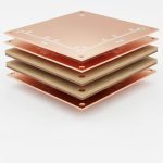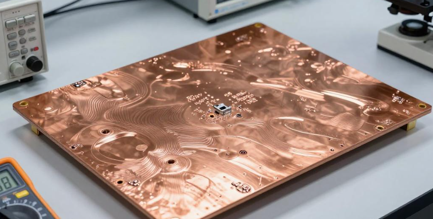
In power-electronics applications such as variable-frequency drives, energy storage systems, and high-power EV charging equipment, engineers often select thick copper PCB designs to handle high-current requirements. Copper weights such as 2 oz, 3 oz, or 4 oz may be considered depending on the electrical and thermal requirements of the application.
However, thicker copper does not always provide the most efficient overall design. As copper thickness increases, PCB fabrication can become more challenging. Greater copper thickness can increase etching difficulty, affect achievable trace width and spacing, increase material usage, and complicate multilayer fabrication. These factors can increase both manufacturing cost and design constraints.
Simply reducing copper thickness to lower cost can create the opposite problem. If the conductor cross-section becomes insufficient, temperature rise and voltage drop may increase, potentially causing thermal stress or power-circuit failure under actual operating conditions.
Therefore, PCB copper thickness reduction should not be treated as a simple material substitution. It is a system-level optimization process involving current-capacity analysis, layout modification, thermal management, manufacturing review, prototype testing, and reliability validation.
The objective is to reduce unnecessary heavy copper while maintaining adequate electrical, thermal, and mechanical performance throughout the expected operating life of the product.
1. Why Optimize Copper Thickness in a Thick Copper PCB?
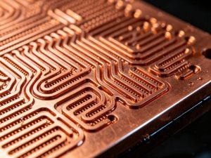
In PCB manufacturing, heavy or thick copper is commonly used when higher current-carrying capability, improved heat spreading, or mechanical robustness is required. However, increasing copper thickness introduces several trade-offs.
One major challenge is etching.
As copper becomes thicker, maintaining accurate trace geometry becomes more difficult because the etching process can produce greater side etching. The final conductor profile may therefore differ significantly from the nominal CAD geometry, particularly when relatively narrow traces are combined with heavy copper.
This can reduce available routing density and make it more difficult to achieve fine trace spacing.
Thick copper can also increase manufacturing complexity during lamination, drilling, plating, and etching. Depending on the stackup and board construction, the additional copper thickness may affect copper balance, resin filling, dimensional stability, and board flatness.
From a cost perspective, heavier copper generally requires more copper material and may involve additional processing requirements. The actual cost impact depends on the PCB structure, copper distribution, production volume, and manufacturer’s process capabilities.
This creates a common optimization opportunity: some designs use the same heavy-copper specification across the entire board even though only a limited number of circuits actually require it.
A power PCB may contain high-current power paths together with low-current control, sensing, and communication circuits. Applying the same heavy-copper requirement to every region can result in unnecessary material and manufacturing costs.
2. Copper Thickness Alone Does Not Determine Current Capacity
One of the most important principles in PCB design is that current-carrying capability is determined by multiple factors rather than copper thickness alone.
Relevant parameters include:
- Copper thickness
- Trace width
- Trace length
- Allowable temperature rise
- Ambient temperature
- Heat dissipation conditions
- PCB layer position
- Copper area
- Via structure
- Adjacent copper planes
- Operating duty cycle
- Continuous and transient current
For a given conductor, increasing trace width can compensate for some reduction in copper thickness because the total conductive cross-sectional area depends on both thickness and width.
For example, a design using 2 oz copper and a relatively narrow power trace might be compared with a 1 oz design using a wider trace. Whether the two configurations provide comparable thermal performance must be determined through engineering analysis rather than assuming a fixed conversion ratio.
A simplified engineering concept is:
Conductor cross-sectional area ≈ copper thickness × effective trace width
However, actual PCB temperature rise is more complex because heat generation and heat dissipation depend on trace geometry, copper planes, board thickness, component heating, airflow, enclosure conditions, and thermal paths.
Therefore, PCB copper thickness reduction should always be evaluated using the complete thermal environment rather than copper cross-sectional area alone.
3. Step One: Use Current-Capacity and Thermal Simulation
The first step in a copper-thickness optimization project is to quantify whether the existing design has sufficient electrical and thermal margin.
Engineers should collect the key operating parameters, including:
- Maximum continuous current
- Peak or transient current
- Ambient temperature
- Operating duty cycle
- Trace width and length
- Existing copper thickness
- PCB layer configuration
- Surface and internal cooling conditions
- Heat-sink or thermal-interface conditions
- Maximum allowable temperature rise
The original design should first be modeled to establish a baseline.
For example, an existing design may use 2 oz copper with a 3 mm power trace carrying a specified continuous current. Engineers can then simulate a candidate design using thinner copper and a wider trace.
The purpose is not to prove that one particular thickness-to-width conversion always works. Instead, the simulation determines whether the proposed geometry can achieve the required temperature rise and voltage-drop limits under the actual operating conditions.
The analysis should also include transient current.
Energy storage systems, motor drives, and power converters may experience short-duration current pulses that are significantly higher than their normal operating current. Even when the average current is relatively moderate, these pulses can create localized heating and electrical stress.
For this reason, the current-carrying capacity evaluation should consider both steady-state and transient operating conditions.
4. Optimize the PCB Layout Together With Copper Thickness
After identifying a potential reduction in copper thickness, the next step is to optimize the physical current path.
Simply changing the copper specification while leaving the original layout unchanged may not provide sufficient margin.
Several layout strategies can be used.
Regional Copper Optimization
A practical approach is to divide the board into functional regions.
High-current power paths, DC buses, switching circuits, and high-power component connections may require larger copper cross-sections. In contrast, low-current control and communication circuits may not require the same copper thickness.
This makes it possible to develop a differentiated copper strategy instead of specifying heavy copper for the entire board.
Depending on the fabrication technology, the design may use different copper constructions in different sections or employ multilayer current sharing to reduce the dependence on a single heavy-copper layer.
Wider Power Traces
When board space permits, increasing trace width can compensate for part of the reduction in copper thickness.
Power traces should avoid unnecessary narrow sections, abrupt width transitions, and localized bottlenecks. Connections between power components and large copper areas should be designed with smooth current transitions.
The actual layout should also consider voltage drop. A trace may meet a temperature requirement while still producing an unacceptable voltage drop because of its resistance.
Large Copper Areas and Thermal Spreading
Large copper areas can help distribute current and spread heat away from high-power components.
For power semiconductors, inductors, connectors, and other heat-generating components, engineers can use appropriately sized copper areas and thermal vias to improve the thermal path.
However, larger copper areas do not automatically solve thermal problems. The heat still needs a complete path from the component through the PCB and, where applicable, into a heat sink, chassis, or airflow.
5. Use Multilayer Current Sharing Where Appropriate
For multilayer PCBs, power distribution can sometimes be improved by using multiple copper layers in parallel.
Instead of requiring one surface trace to carry the entire current, two or more appropriately connected copper layers can share the current.
This approach can increase the effective conductive area while allowing the copper thickness of an individual layer to be reduced.
However, effective current sharing depends on the interconnection structure.
Via quantity, via diameter, via placement, copper-plane geometry, connection resistance, and current distribution all influence how evenly current is shared between layers.
A few vias placed at one end of a power path should not automatically be assumed to provide uniform current distribution.
For high-current applications, engineers should evaluate the complete current path, including:
Component Pad → Copper Trace → Via Array → Internal Plane → Via Array → Output Connection
This approach can also reduce localized current density and improve thermal spreading.
6. Consider High-Frequency Effects During Copper Optimization
Copper-thickness optimization becomes more complicated when the board contains high-frequency switching circuits.
For predominantly DC current paths, conventional resistance and temperature-rise calculations may provide a useful starting point.
For switching power circuits, however, the current waveform may contain significant AC components. Frequency-dependent resistance, skin effect, proximity effect, parasitic inductance, and current-loop geometry can then influence power loss.
A thicker conductor does not always provide a proportional improvement in high-frequency performance.
Therefore, when optimizing copper thickness for switching converters, engineers should also examine:
- Switching frequency
- Ripple current
- Current-loop area
- Return-path geometry
- High-frequency capacitor placement
- Parasitic inductance
- AC conduction losses
- Electromagnetic coupling
In some cases, reducing loop area and improving component placement can provide greater benefits than simply increasing copper thickness.
This is particularly important for inverter and high-frequency power-conversion applications.
7. DFM Review Is Essential Before Fabrication
After the electrical and thermal optimization is complete, the revised design should undergo a DFM review.
The purpose is to verify that the proposed geometry can be manufactured consistently at the required production volume.
The review should cover:
- Minimum trace width
- Trace spacing
- Copper-to-edge clearance
- Copper balance
- Drill and via dimensions
- Plating requirements
- Solder-mask clearance
- Pad-to-trace transitions
- Copper distribution
- Lamination structure
- Warpage risk
- Etching capability
Reducing copper thickness may improve etching capability and routing density, but widening power traces can consume additional PCB area.
Therefore, the final design should balance copper thickness, trace width, board size, electrical performance, and manufacturing capability.
A design that works well in simulation may still require modification if its geometry creates manufacturing difficulties.
8. Prototype Testing: Verify the Real Thermal Performance
After completing the DFM review, prototype boards should be manufactured and tested under representative operating conditions.
Where possible, engineers should compare the original thick-copper design with the optimized design using the same test equipment and test conditions.
Important measurements include:
- Full-load temperature rise
- Dynamic-load temperature response
- Thermal imaging
- DC voltage drop
- Conductor resistance
- Component temperature
- Connector temperature
- Via-region temperature
- Power-loss comparison
Thermal imaging is especially useful for identifying localized hot spots.
The hottest point may not be located in the center of a wide trace. It may appear near a via transition, component pad, connector, narrow neck, or current-sharing junction.
Testing should therefore focus on critical current-density locations rather than measuring only one point on the PCB.
9. Reliability Testing After Copper Thickness Reduction
Short-term load testing is necessary but may not be sufficient to establish long-term reliability.
After the optimized design passes electrical and thermal testing, an appropriate PCB reliability validation program should be established according to the product application and applicable requirements.
Depending on the product, testing may include:
- Long-duration full-load aging
- Temperature cycling
- High-temperature exposure
- Humidity testing
- Repeated load cycling
- Electrical insulation testing
- Post-aging resistance measurement
- Post-aging temperature-rise testing
The objective is to determine whether the optimized PCB retains sufficient electrical and thermal margin after prolonged stress.
Engineers should compare key parameters before and after aging, including conductor resistance, voltage drop, temperature rise, and the location of thermal hot spots.
Reliability evaluation should also consider solder joints, vias, connectors, component interfaces, and other parts of the current path.
10. Define Clear Boundaries for Copper Thickness Reduction
Not every application is suitable for aggressive copper-thickness reduction.
Extra caution is required when the product has:
- Extremely high continuous current
- Very high peak current
- Limited routing space
- High ambient temperature
- Poor enclosure ventilation
- Severe thermal constraints
- High-frequency switching currents
- Strict voltage-drop requirements
- Long operating cycles
- High reliability requirements
In these applications, the available thermal and electrical margin may be too small to justify a substantial reduction in copper thickness.
Engineers should also consider product aging and manufacturing variation. The optimized design should retain sufficient margin to accommodate reasonable variation in material properties, copper thickness, trace dimensions, operating conditions, and production processes.
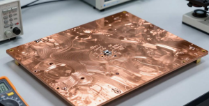
11. Kingda’s Role in Copper Thickness Optimization
For power-electronics applications, Kingda can support the transition from a heavy-copper concept to a manufacturable and validated PCB design.
The optimization process can integrate electrical requirements, layout considerations, DFM analysis, material selection, copper distribution, plating requirements, prototype fabrication, and production quality control.
The goal is not simply to reduce copper usage. Instead, the objective is to determine where heavy copper is genuinely necessary and where alternative design measures can provide sufficient electrical and thermal performance.
By combining appropriate trace geometry, copper-plane distribution, thermal management, multilayer current sharing, and manufacturing analysis, engineers can potentially reduce unnecessary heavy-copper processing while maintaining product reliability.
Conclusion
PCB copper thickness reduction is not simply a matter of replacing a thick copper foil with a thinner one.
For power-electronics PCBs, copper thickness must be evaluated together with trace width, current density, thermal conditions, transient current, high-frequency effects, layer structure, and manufacturing capability.
A practical optimization workflow is:
Requirement Analysis → Current-Capacity Simulation → PCB Design Optimization → Thermal Analysis → DFM Review → Prototype Fabrication → Load Testing → Reliability Validation → Mass-Production Control
The most effective solution is often a combination of moderate copper thickness, optimized power-trace geometry, appropriate copper-plane distribution, improved thermal management, and carefully designed current paths.
With a systematic approach, engineers can reduce unnecessary heavy-copper usage, improve manufacturing flexibility, control PCB cost, and maintain the electrical and thermal performance required for demanding power-electronics applications.