4-Layer PCB Stackup: PCB Design, PCB Manufacturing & Layer Stackup Guide
A proper PCB stackup is one of the most important considerations in multilayer PCB design. Its importance becomes particularly evident when designing four-layer and higher-layer-count printed circuit boards. Among multilayer configurations, the four-layer PCB is one of the most widely used because it provides a practical balance between routing density, signal integrity, power distribution, manufacturability, and cost.
The design rules and layer configuration of a four-layer PCB differ significantly from those of a two-layer PCB. Ignoring these differences can lead to unnecessary manufacturing costs, poor signal integrity, electromagnetic compatibility (EMC) problems, and even PCB defects. Therefore, understanding the standard four-layer PCB stackup is essential for engineers, designers, and purchasing teams involved in PCB Manufacturing.
What Is a 4-Layer PCB Stackup?
A typical four-layer PCB stackup consists of four copper layers separated by dielectric materials. The two outer copper layers are normally used for component placement and signal routing, while the two inner copper layers are commonly assigned to ground and power distribution.
A typical arrangement is:
- Top Copper Layer – Signal and Component Layer
- Dielectric Layer
- Inner Copper Layer – Ground Plane
- Core / Dielectric Layer
- Inner Copper Layer – Power Plane
- Dielectric Layer
- Bottom Copper Layer – Signal and Component Layer
Although this is a common arrangement, the exact configuration should be selected according to the electrical, mechanical, thermal, and manufacturing requirements of the product.
The popularity of four-layer PCBs comes largely from their ability to provide more routing space and better power integrity than two-layer boards without the manufacturing complexity and cost associated with higher layer counts.
In high-speed applications, the stackup also plays an important role in controlling impedance, minimizing signal reflections, reducing electromagnetic interference (EMI), and providing predictable return-current paths.
The arrangement, thickness, and material properties of the copper and dielectric layers collectively define the PCB stackup. A properly engineered stackup is therefore fundamental to achieving reliable PCB Design, signal integrity, EMC performance, and power management.
For production, the finalized stackup should be clearly communicated to the manufacturer through fabrication documentation, stackup drawings, material specifications, and impedance requirements.
Main Layers of a 4-Layer PCB
A standard four-layer PCB typically contains the following functional layers.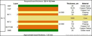
1. Top Copper Layer
The top copper layer is normally the primary component placement and signal-routing layer. Most components are placed on this side because assembling components on a single side can simplify the SMT assembly process and reduce manufacturing costs.
For many four-layer PCB designs, the top layer is also preferred for high-speed signals because it can be routed directly above a continuous ground reference plane.
- When impedance-controlled traces are required, the distance between the top copper layer and its reference plane becomes particularly important. Trace width, copper thickness, dielectric thickness, dielectric constant, and the surrounding copper geometry all affect controlled impedance.
If high-speed signals are routed on the top layer, unnecessary power routing on the same layer should generally be avoided. Keeping the high-speed routing environment clean helps maintain a predictable electromagnetic field and return-current path.
2. Top Dielectric Layer
The dielectric layer directly below the top copper layer electrically separates the signal layer from the inner copper plane.
Depending on the manufacturer’s stackup construction, this dielectric region may be formed by prepreg, core material, or a combination of materials.
Its thickness is especially important for impedance-controlled traces. A smaller distance between the signal trace and its reference plane generally produces stronger electromagnetic coupling and affects the resulting characteristic impedance.
Therefore, during PCB Design, engineers should not select trace widths independently of the stackup. The dielectric thickness and material properties should be determined first, followed by impedance calculations and trace geometry optimization.
3. Second Copper Layer
The second copper layer is an inner copper layer and is commonly assigned as a continuous ground plane in a four-layer PCB.
For high-speed designs, maintaining a solid ground reference directly beneath the top signal layer provides a short and predictable return-current path. This can significantly improve signal integrity and reduce unwanted electromagnetic radiation.
The second layer should generally not be heavily fragmented by unnecessary signal routing, particularly in areas containing high-speed or impedance-controlled signals.
For designs that do not contain demanding high-speed interfaces, portions of this layer may be allocated differently. However, using an inner layer as a dedicated ground plane is often an effective strategy for improving overall electrical performance.
For power electronics, this layer can also contribute to power and ground distribution depending on the current requirements and thermal design.
4. Middle Dielectric Layer
The middle dielectric region separates the two internal copper layers and contributes significantly to the overall thickness and mechanical structure of the PCB.
Its thickness is determined by several factors, including:
- Overall PCB thickness
- Required dielectric spacing
- Impedance requirements
- Voltage isolation requirements
- Material selection
- Manufacturing capabilities
- Thermal and mechanical requirements
A relatively thick dielectric layer between internal copper planes can provide greater electrical isolation. However, increasing dielectric thickness does not automatically improve every aspect of PCB performance.
For a standard four-layer PCB, the stackup should ideally be designed with manufacturing capability and material availability in mind. Excessively customized dielectric thicknesses can increase fabrication complexity and cost.
5. Third Copper Layer
The third copper layer is adjacent to the bottom copper layer, so its function depends largely on the type of routing used on the bottom layer.
If the bottom layer carries high-speed signals, the third copper layer should generally serve as a continuous ground reference plane. This arrangement provides the high-speed signals with a controlled return path and helps maintain signal integrity.
If the bottom layer is primarily used for general-purpose signals, the third copper layer may instead be used for power distribution, which is common in many four-layer PCB stackups.
Some applications may require selected signal networks to be routed through this layer. However, impedance-controlled signals should not be routed on this layer without carefully considering the available reference plane, dielectric spacing, trace geometry, and return-current path.
For demanding high-speed applications, maintaining a continuous reference plane is generally more important than maximizing routing space on every internal layer.
6. Bottom Dielectric Layer
The bottom dielectric layer separates the third copper layer from the bottom copper layer.
Its electrical role is similar to that of the dielectric layer between the top copper and second copper layers. Its thickness and dielectric properties directly affect the impedance of traces routed on the bottom layer.
For a symmetrical four-layer PCB stackup, the dielectric construction on the top and bottom sides may be designed to provide balanced mechanical characteristics.
Symmetry can also help reduce mechanical deformation during PCB manufacturing, particularly when copper distribution and dielectric thickness are properly balanced.
7. Bottom Copper Layer
The bottom copper layer can be used for signal routing, power distribution, and, depending on the product architecture, component placement.
In many conventional designs, most components are placed on the top side to simplify assembly. Nevertheless, bottom-side components can be useful when space is limited or when the product requires higher component density.
The bottom layer can also carry high-speed signals if the third copper layer provides an appropriate continuous ground reference.
In a typical four-layer PCB, bottom-layer routing may use vias to connect to other signal layers. However, designers should avoid excessive via transitions in high-speed signal paths because discontinuities can affect impedance and signal integrity.
For a symmetrical stackup, the top and bottom copper layers are often designed with similar copper thicknesses, although the exact values depend on current-carrying requirements and manufacturing constraints.
Ideal 4-Layer PCB Stackup
There is no single four-layer PCB stackup that is ideal for every application. The optimal configuration depends on signal speed, power requirements, impedance targets, component density, thermal requirements, PCB thickness, and manufacturing capabilities.
A commonly used configuration is:
| Layer | Typical Function |
|---|---|
| L1 – Top Copper | Components + high-speed/general signal routing |
| L2 – Inner Copper | Continuous ground plane |
| L3 – Inner Copper | Power plane / power distribution |
| L4 – Bottom Copper | General signal routing + selected components |
This arrangement provides a relatively straightforward routing architecture and gives the top layer a dedicated ground reference.
For high-speed applications, another strategy is to configure both internal layers primarily as reference planes or to dedicate one plane to ground and the other to power, depending on the required routing architecture.
The dielectric materials between the copper layers should then be selected based on impedance, voltage isolation, thickness, cost, and availability.
Why Ground and Power Planes Matter
Ground planes and power planes are not simply additional copper areas. They play an important role in electrical performance.
A continuous ground plane can:
- Provide a low-impedance return-current path
- Reduce loop area
- Improve signal integrity
- Reduce EMI
- Support controlled-impedance routing
- Improve power integrity
Power planes can also reduce distribution resistance and inductance when appropriately designed.
For this reason, the layer assignment should be determined early in the PCB Design process rather than after routing has already been completed.
4-Layer PCB Stackup for High-Speed Signals
High-speed PCB design requires greater attention to stackup geometry than conventional low-speed circuits.
A high-speed signal should ideally have a continuous reference plane directly adjacent to its routing layer. The shorter the distance between the trace and its reference plane, the more tightly controlled the electromagnetic field tends to be.
Important factors include:
- Trace width
- Copper thickness
- Dielectric thickness
- Dielectric constant
- Reference-plane continuity
- Via transitions
- Differential-pair spacing
- Signal rise time
- Target impedance
For differential interfaces such as USB, Ethernet, PCIe, LVDS, and other high-speed protocols, designers should calculate the required differential impedance based on the actual stackup rather than relying on generic trace-width recommendations.
When a high-speed trace changes layers through a via, its return current must also transition between reference planes. Ground stitching vias and appropriate plane transitions can help provide a continuous return path.
4-Layer PCB Stackup and Impedance Control
Controlled impedance is particularly important when a PCB contains high-speed digital, RF, or other sensitive interfaces.
The characteristic impedance of a PCB trace is influenced by the relationship between the trace and its reference plane.
For a microstrip structure on an outer layer, the major parameters include:
- Trace width
- Copper thickness
- Dielectric height
- Dielectric constant
For an internal stripline structure, the trace is embedded between reference planes, and both dielectric spacing and material properties influence the impedance.
Therefore, designers should obtain the manufacturer’s actual stackup before finalizing impedance-controlled routing.
A manufacturer such as Kingda can use the required board thickness, copper thickness, dielectric materials, layer arrangement, and impedance targets to establish a manufacturable stackup.
Important Considerations for 4-Layer PCB Stackup Design
Consult the PCB Manufacturer Early
One of the most effective ways to reduce unnecessary manufacturing costs is to consult the manufacturer before finalizing the stackup.
Experienced PCB manufacturers can provide recommendations based on standard materials, available copper thicknesses, standard dielectric constructions, fabrication capabilities, and impedance requirements.
Using a manufacturer’s standard stackup can improve manufacturability and reduce the risk of unexpected fabrication costs.
If a PCB stackup requires unusual materials or non-standard dielectric thicknesses, the manufacturer may need additional processing steps or special materials. These requirements can increase both cost and production lead time.
For this reason, working with a qualified PCB Manufacturing partner during the design stage can prevent expensive redesigns later in the project.
Choose Dielectric Materials Carefully
Dielectric material selection affects electrical, thermal, mechanical, and manufacturing performance.
Common considerations include:
- Dielectric constant (Dk)
- Dissipation factor (Df)
- Thermal resistance
- Glass-transition temperature (Tg)
- Coefficient of thermal expansion (CTE)
- Moisture resistance
- Cost
- Availability
For standard four-layer PCBs, conventional FR-4 materials are often sufficient. More demanding applications may require specialized low-loss or high-frequency laminates.
Using premium materials without a technical requirement can unnecessarily increase PCB cost, while using unsuitable materials can compromise signal integrity and reliability.
Do Not Simply Add Layers
Increasing a PCB from two layers to four layers should not be treated as simply duplicating the existing routing layout.
If a two-layer PCB has insufficient routing space, designers should first consider component placement, routing optimization, board dimensions, and functional partitioning.
When upgrading to four layers, it is often better to redesign the stackup and layout architecture from the beginning.
A four-layer PCB provides more than additional routing space. It allows engineers to establish dedicated power and ground structures, improve signal-return paths, reduce routing congestion, and create a more compact and reliable design.
Maintain a Clear Stackup in Manufacturing Documentation
The final stackup should be clearly documented in the PCB fabrication package.
Although a separate stackup drawing may not always be mandatory, providing one significantly reduces the possibility of communication errors between the PCB designer and manufacturer.
A typical stackup document can specify:
- Number of PCB layers
- Copper thickness
- Dielectric materials
- Dielectric thickness
- Finished board thickness
- Surface finish
- Controlled impedance requirements
- Material specifications
- Layer functions
- Manufacturing tolerances
The Gerber files define the physical artwork for individual layers, but they do not by themselves communicate every manufacturing requirement. Therefore, the fabrication drawing and manufacturing notes should complement the Gerber data.
4-Layer PCB Stackup and Gerber Files
A complete PCB manufacturing package normally contains more than Gerber files.
Depending on the project, documentation may include:
- Gerber or other fabrication data
- Drill files
- Stackup information
- Fabrication drawing
- Assembly drawing
- Bill of materials (BOM)
- Pick-and-place data
- Impedance requirements
- Surface-finish specifications
- Special manufacturing instructions
Maintaining consistent layer naming between the PCB CAD design, fabrication documentation, and manufacturing data is particularly important.
For example, the designer should ensure that the layer identified as the ground plane in the stackup corresponds correctly to the physical layer represented in the fabrication data.
Good documentation helps prevent layer-order mistakes, material substitutions, and manufacturing misunderstandings.
Common 4-Layer PCB Stackup Mistakes
Several mistakes frequently affect four-layer PCB performance and manufacturability.
Fragmenting the Ground Plane
Routing signals through or unnecessarily dividing a reference plane can interrupt return-current paths. This can increase loop area and create signal-integrity or EMI problems.
Ignoring the Actual Manufacturer Stackup
Using generic impedance calculations without confirming the actual dielectric thickness and material properties can result in incorrect trace impedance.
Excessive Via Transitions
Every via introduces a physical discontinuity. High-speed signals should use carefully planned layer transitions to minimize impedance discontinuities and return-path problems.
Poor Copper Balance
Uneven copper distribution across the PCB can contribute to warpage and manufacturing difficulties. Copper balance should therefore be considered during both layout and fabrication planning.
Treating Power Routing Like Ordinary Signal Routing
Power distribution has different requirements from ordinary signal routing. Current capacity, voltage drop, thermal performance, and plane impedance should all be considered when assigning power layers.
How to Design a Reliable 4-Layer PCB Stackup
A practical design workflow can follow these steps:
Step 1: Define electrical requirements
Determine signal speeds, interface types, target impedance, operating voltage, current requirements, and EMC requirements.
Step 2: Define mechanical requirements
Determine the board dimensions, finished thickness, mounting requirements, connector locations, and enclosure constraints.
Step 3: Select the layer architecture
Decide which layers will be used for signals, ground, and power.
Step 4: Select appropriate materials
Choose core and prepreg materials according to electrical, thermal, mechanical, and cost requirements.
Step 5: Confirm the stackup with the manufacturer
Verify that the proposed stackup uses practical and available materials and manufacturing processes.
Step 6: Calculate controlled impedance
Use the confirmed dielectric thickness, copper thickness, and material properties to calculate trace widths and spacing.
Step 7: Complete PCB routing
Route high-speed signals over continuous reference planes and minimize unnecessary layer transitions.
Step 8: Perform design verification
Conduct DRC, signal-integrity analysis, impedance verification, power-integrity analysis, and manufacturability checks as required.
Step 9: Release complete manufacturing documentation
Provide Gerber files, drill data, stackup information, fabrication drawings, and all other necessary manufacturing instructions.
4-Layer PCB Stackup: PCB Design and PCB Manufacturing
A well-designed four-layer PCB stackup provides the foundation for reliable electrical performance and efficient manufacturing. The layer arrangement affects routing density, signal integrity, impedance control, power distribution, EMI performance, thermal behavior, and overall production cost.
For standard applications, a common approach is to use the top and bottom copper layers for signal routing, maintain a solid ground plane on one inner layer, and use the remaining inner layer for power distribution. However, high-speed, RF, high-current, and other specialized applications may require a different architecture.
The most important principle is that the stackup should be designed before routing, not after the PCB layout has been completed. Engineers should establish the electrical and mechanical requirements first, select an appropriate material system, verify the stackup with the PCB manufacturer, and then perform impedance-controlled routing.
For companies looking for reliable PCB Manufacturing and PCB assembly support, Kingda can provide engineering assistance for stackup planning, DFM review, fabrication, assembly, and testing. Working with the manufacturer early in the design process can help reduce unnecessary redesigns, improve manufacturability, and support consistent production quality.
Conclusion
The 4-layer PCB stackup is much more than a simple arrangement of copper and dielectric layers. It is a fundamental part of the electrical and mechanical architecture of the entire circuit board.
A properly designed stackup can provide continuous reference planes, controlled impedance, reliable power distribution, improved signal integrity, better EMC performance, and more predictable manufacturing results.
For standard four-layer PCB projects, designers should prioritize a practical and manufacturer-friendly stackup rather than selecting a complex configuration without a clear technical requirement. For high-speed or specialized applications, stackup design should be closely coordinated with impedance calculations, signal-integrity analysis, material selection, and fabrication capabilities.
By integrating PCB Design and PCB Manufacturing considerations from the beginning, engineers can create four-layer PCBs that are not only electrically reliable but also cost-effective and easier to manufacture at scale.
Article Summary
A 4-layer PCB stackup typically combines two outer signal layers with two inner copper layers used primarily for ground and power distribution. The correct arrangement of copper, core, and prepreg materials directly affects impedance control, signal integrity, EMC, power integrity, mechanical stability, and manufacturing cost. Before routing begins, engineers should define the electrical requirements, select a practical stackup, confirm the construction with the PCB manufacturer, and document the final configuration in the fabrication package. For reliable PCB Design and PCB Manufacturing, a well-engineered four-layer stackup provides a strong foundation for both prototype development and volume production.