Immersion Gold PCB Surface Finish: PCB Design, PCB Manufacturing & ENIG Guide
The electronics industry has become an essential part of modern life because of our growing dependence on computers, smartphones, data-storage systems, industrial machines, automotive electronics, and other connected devices. Modern electronic products process information at increasingly high speeds, significantly reducing waiting times while offering smaller dimensions, lower weight, and greater portability.
At the heart of many of these products is the printed circuit board (PCB), which mechanically supports electronic components and provides the electrical interconnections required for the system to function.
A PCB consists of dielectric materials, conductive copper traces, pads, planes, and vias. Because exposed copper can oxidize and degrade when exposed to moisture, contaminants, and environmental conditions, an appropriate surface finish is required on exposed copper areas.
Common PCB surface finishes include Organic Solderability Preservative (OSP), Hot Air Solder Leveling (HASL), immersion tin, immersion silver, and gold-based finishes.
Among these technologies, Immersion Gold PCB surface finishes are widely used when excellent surface flatness, solderability, oxidation resistance, and long-term reliability are required.
However, “immersion gold” can refer to several related but technically different gold-finish systems. ENIG (Electroless Nickel Immersion Gold) and ENEPIG (Electroless Nickel Electroless Palladium Immersion Gold) are two important examples. Understanding these differences is essential when selecting a surface finish during PCB Design and PCB Manufacturing.
What Is an Immersion Gold PCB Surface Finish?
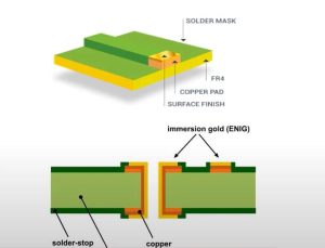
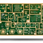
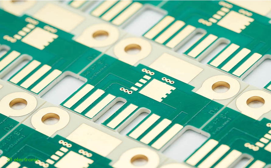
An Immersion Gold PCB surface finish is a gold-containing surface treatment in which a thin layer of gold is deposited onto an underlying metallic surface.
In conventional ENIG construction, the gold is deposited over an electroless nickel layer rather than directly onto bare copper. The nickel provides a protective barrier and mechanical foundation, while the thin immersion-gold layer protects the nickel surface and provides a solderable contact surface.
The gold layer itself is very thin. Its primary purpose is not to provide a thick structural coating but to protect the underlying surface and maintain suitable solderability and contact performance.
Depending on the required application, manufacturers may use different gold-based surface finishes, including:
- ENIG — Electroless Nickel Immersion Gold
- ENEPIG — Electroless Nickel Electroless Palladium Immersion Gold
- Hard gold/electroplated gold for selected contact areas
- Other specialized gold-based finishes
These finishes should not be treated as interchangeable because their layer structures, manufacturing processes, mechanical characteristics, and applications are different.
What Are the Advantages of Immersion Gold PCB Surface Finish?
Compared with finishes such as HASL or OSP, gold-based surface finishes can have a higher manufacturing cost. Nevertheless, they are widely selected for applications where surface flatness, solderability, oxidation resistance, and contact reliability are important.
1. Excellent Oxidation Resistance
Gold is a noble metal with high resistance to oxidation under normal environmental conditions.
A properly controlled immersion-gold surface protects the underlying metallic surface from direct environmental exposure and helps maintain a stable solderable surface during storage and assembly.
This characteristic is particularly useful when PCBs need to be stored for longer periods before assembly.
2. Good Solderability
A properly manufactured gold-based surface finish provides a clean and relatively flat surface for soldering.
For ENIG, the thin immersion-gold layer protects the nickel surface before assembly. During soldering, the gold dissolves into the solder, allowing the soldering process to interact primarily with the underlying nickel layer.
This makes ENIG particularly useful for fine-pitch components and surface-mount assemblies where consistent pad geometry is important.
3. Excellent Surface Flatness for Fine-Pitch Components
One of the major reasons manufacturers select ENIG is its relatively flat surface.
Unlike HASL, which can produce variations in solder coating thickness, ENIG provides a more uniform surface suitable for fine-pitch component assembly.
This is especially valuable for:
- BGA packages
- QFN packages
- Fine-pitch ICs
- Micro-BGA packages
- High-density SMT assemblies
Therefore, surface-finish selection should be considered during PCB Design, especially when the board contains fine-pitch components.
4. Good Storage Stability
Because gold has excellent resistance to oxidation, ENIG and other properly controlled gold-based finishes can provide good storage characteristics.
This can be beneficial when PCB fabrication and assembly occur at different locations or when boards need to remain in inventory before assembly.
However, proper packaging and storage conditions are still necessary. A gold finish does not eliminate all contamination, handling, or environmental risks.
5. Suitable for High-Reliability Applications
Gold-based finishes are commonly used in applications where reliable soldering and stable surface characteristics are important.
These include:
- Automotive electronics
- Medical electronics
- Industrial controls
- Telecommunications equipment
- Networking equipment
- Consumer electronics
- High-density computing hardware
The actual suitability of a surface finish depends on the complete design, material system, assembly process, reliability requirements, and applicable industry standards.
How Does Immersion Gold PCB Surface Treatment Work?
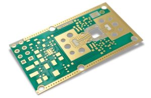
Several gold-based PCB surface finishes are available, but their manufacturing processes are not identical.
It is therefore important to distinguish between immersion gold, ENIG, and ENEPIG.
Electroless Nickel Immersion Gold (ENIG)
ENIG is one of the most widely used gold-based PCB surface finishes.
Its basic structure is:
Copper → Electroless Nickel → Immersion Gold
The copper surface is first prepared for electroless nickel deposition. A nickel layer is then deposited chemically without applying an external electrical current.
After the nickel layer has been formed, the PCB enters an immersion-gold bath. Through a displacement reaction, a thin layer of gold is deposited onto the exposed nickel surface.
The resulting gold layer is thin, while the nickel layer provides the primary barrier between the copper and the external environment.
Electroless Nickel Electroless Palladium Immersion Gold (ENEPIG)
ENEPIG adds a palladium layer between nickel and gold:
Copper → Electroless Nickel → Electroless Palladium → Immersion Gold
The palladium layer acts as an additional barrier and can improve compatibility with certain demanding assembly and contact applications.
ENEPIG is often selected when a broader combination of soldering and bonding requirements must be supported, although it generally involves greater process complexity and cost than conventional ENIG.
Electroplated Gold
Electroplated gold is different from immersion gold.
Electroplated gold uses an externally applied electrical current to deposit gold onto selected conductive areas. Depending on the application, thicker hard-gold coatings may be used for edge connectors, contact fingers, switches, and other wear-resistant electrical contacts.
Therefore, electroplated hard gold should not be described simply as immersion gold.
What Are the Steps in the ENIG PCB Process?
The exact process parameters vary between manufacturers and material systems, but a typical ENIG process includes the following stages.
1. Surface Cleaning
The copper surface is thoroughly cleaned to remove oil, oxides, dust, fingerprints, and other contaminants.
A clean surface is essential because contamination can interfere with subsequent chemical reactions and lead to uneven deposition.
2. Micro-Etching
The copper surface may undergo controlled micro-etching to remove surface oxides and prepare the copper for the subsequent chemical treatment.
The process must be carefully controlled because excessive copper removal can affect dimensional accuracy and pad geometry.
3. Surface Activation
The copper surface is chemically activated to enable the electroless nickel deposition process.
Activation must be uniform across the panel to support consistent nickel coverage.
4. Electroless Nickel Deposition
The PCB is immersed in an electroless nickel bath.
Unlike electrolytic plating, electroless nickel deposition does not require the PCB to function as an electrode connected to an external power supply.
The nickel layer provides several important functions:
- Acts as a diffusion barrier
- Protects the underlying copper
- Provides mechanical support for the gold finish
- Creates the surface onto which immersion gold is deposited
5. Immersion Gold Deposition
After nickel deposition, the PCB is transferred to the immersion-gold bath.
A controlled chemical displacement reaction deposits a thin layer of gold over the exposed nickel.
The gold thickness must be carefully controlled because the purpose of immersion gold is primarily surface protection and solderability rather than forming a thick structural gold coating.
6. Rinsing and Drying
The PCB is thoroughly rinsed to remove chemical residues and then dried.
Proper rinsing is important because residual process chemicals can affect surface quality and long-term reliability.
7. Inspection and Testing
The finished surface is inspected to verify:
- Surface uniformity
- Pad appearance
- Nickel coverage
- Gold coverage
- Surface cleanliness
- Thickness compliance
- Solderability
- Other application-specific requirements
Thickness measurements can be performed using appropriate analytical or non-destructive techniques depending on the required control level.
ENIG vs. ENEPIG: What Is the Difference?
ENIG and ENEPIG are two important gold-based PCB surface finishes, but their structures differ.
| Feature | ENIG | ENEPIG |
|---|---|---|
| Basic structure | Copper / Nickel / Gold | Copper / Nickel / Palladium / Gold |
| Nickel layer | Yes | Yes |
| Palladium layer | No | Yes |
| Gold layer | Yes | Yes |
| Process complexity | Lower | Higher |
| Relative cost | Generally lower | Generally higher |
| Surface flatness | Excellent | Excellent |
| Typical applications | Fine-pitch SMT, BGA, general high-reliability PCBs | Advanced packaging, demanding assembly and contact applications |
The choice should be based on the complete application rather than assuming that one finish is universally better.
Immersion Gold vs. HASL vs. OSP
Different surface finishes provide different combinations of cost, solderability, flatness, storage stability, and manufacturing complexity.
| Surface Finish | Main Advantages | Typical Considerations |
|---|---|---|
| ENIG | Flat surface, good solderability, oxidation resistance | Higher cost than some conventional finishes |
| ENEPIG | Excellent flatness and versatile surface performance | Higher process complexity and cost |
| HASL | Established process, economical for many applications | Less suitable for extremely fine-pitch applications |
| OSP | Low cost, flat copper surface, lead-free compatible | Surface is more sensitive to handling and storage conditions |
| Immersion Silver | Flat surface and good solderability | Requires appropriate handling and storage |
| Immersion Tin | Flat surface and suitable solderability | Requires careful process and storage control |
There is no single surface finish that is optimal for every PCB.
The correct choice depends on component pitch, assembly technology, storage requirements, electrical requirements, reliability targets, environmental conditions, and cost.
What Are the Applications of Immersion Gold PCBs?
Gold-based PCB surface finishes are used across a wide range of electronic products.
Consumer Electronics
Gold-based finishes are commonly found in products requiring compact layouts and fine-pitch SMT assembly, including:
- Smartphones
- Wearable devices
- Tablets
- Laptops
- Portable electronics
- Networking equipment
For high-density consumer electronics, the flatness of ENIG can be particularly useful for BGA and fine-pitch component assembly.
Automotive Electronics
Automotive electronic systems operate under demanding environmental conditions, including temperature cycling, vibration, humidity, and long operating lifetimes.
Gold-based surface finishes may be selected for automotive PCBs where reliable solderability and controlled surface characteristics are required.
Applications can include:
- Automotive control units
- Infotainment systems
- ADAS electronics
- Battery-management systems
- Vehicle communication modules
- Sensor electronics
However, the surface finish is only one part of automotive PCB reliability. Material selection, copper structure, via reliability, soldering processes, cleanliness, and qualification requirements must also be considered.
Medical Electronics
Medical equipment places strong emphasis on reliability, consistency, traceability, and manufacturing quality.
Gold-based finishes can be used in medical PCB assemblies where stable solderability and fine-pitch assembly are required.
Potential applications include:
- Patient monitoring equipment
- Diagnostic instruments
- Medical imaging electronics
- Portable medical devices
- Laboratory equipment
The specific surface finish should be selected according to the device’s electrical, mechanical, environmental, regulatory, and assembly requirements.
Telecommunications and Networking
High-density communication hardware frequently uses multilayer PCBs with fine-pitch components and controlled-impedance structures.
The flat surface provided by ENIG can support high-density SMT assembly and BGA packages, making it suitable for many communication and networking applications.
Industrial Electronics
Industrial controllers, instrumentation, automation systems, power-management equipment, and other industrial electronics may also use gold-based surface finishes when reliability and surface stability are important.
How to Choose the Right PCB Surface Finish
When selecting a surface finish during PCB Design, engineers should evaluate several factors rather than focusing only on initial manufacturing cost.
Component Pitch
Fine-pitch components and BGA packages generally benefit from flat and uniform pad surfaces.
Assembly Process
The selected finish must be compatible with the soldering process, component package, and assembly conditions.
Storage Requirements
If the PCB will be stored for extended periods before assembly, surface oxidation resistance becomes increasingly important.
Reliability Requirements
Automotive, medical, industrial, aerospace, and telecommunications products may require more demanding reliability specifications than ordinary consumer products.
Cost
Surface finish can represent a meaningful portion of PCB fabrication cost. The appropriate finish should balance performance requirements with the overall product cost target.
Manufacturing Capability
Not every PCB manufacturer has identical process capability. Engineers should confirm that the selected supplier can consistently achieve the required nickel and gold thickness, surface quality, pad geometry, and reliability.
PCB Design Considerations for ENIG
The surface finish should be considered during the design stage rather than being treated as an afterthought.
Important design considerations include:
- Pad dimensions
- Component pitch
- BGA land patterns
- Solder mask clearance
- Copper thickness
- Controlled impedance
- Via-in-pad requirements
- Surface-finish specifications
- Required gold and nickel thickness
- Assembly process
- Reliability requirements
For advanced PCB assemblies, close communication between the designer, PCB manufacturer, and assembly provider can reduce manufacturing risks.
A manufacturer such as Kingda can review the design and manufacturing requirements before production to help ensure that the selected surface finish is compatible with the board structure and assembly process.
Common Problems With Gold-Based PCB Finishes
Although ENIG and other gold-based finishes provide many advantages, manufacturing quality remains critical.
Potential issues include:
Black Pad
Black pad is a well-known ENIG-related reliability concern associated with certain nickel surface conditions and excessive or uncontrolled corrosion during the immersion-gold process.
Proper chemistry control, process monitoring, and inspection are essential for minimizing this risk.
Uneven Coating
Insufficient surface preparation or unstable chemical conditions can produce non-uniform nickel or gold deposition.
Excessive Gold Thickness
Immersion gold is intended to be a relatively thin protective finish. Excessive gold can affect soldering behavior and increase cost.
Poor Surface Cleanliness
Contamination before or after surface finishing can affect solderability and long-term reliability.
For this reason, PCB surface-finish quality depends not only on material selection but also on strict process control.
Conclusion
Immersion Gold PCB surface finishing is an important technology for modern electronics where surface flatness, solderability, oxidation resistance, and reliability are important.
Among gold-based finishes, ENIG PCB technology is widely used because its nickel-gold structure provides a flat and stable surface suitable for fine-pitch SMT, BGA, and many high-density PCB assemblies. ENEPIG adds a palladium layer and can be considered for applications with more demanding assembly or contact requirements.
However, immersion gold, ENIG, ENEPIG, and electroplated hard gold are not identical processes. Their structures, deposition mechanisms, performance characteristics, and applications must be clearly distinguished when selecting a PCB surface finish.
For successful PCB Design and PCB Manufacturing, engineers should evaluate component pitch, assembly technology, storage conditions, reliability requirements, environmental exposure, manufacturing capability, and cost before selecting the appropriate surface finish.
Working with an experienced manufacturer such as Kingda can help ensure that surface-finish requirements are properly integrated into the PCB fabrication process and that the finished boards meet the intended electrical, mechanical, and assembly requirements.
Article Summary
This article explains Immersion Gold PCB surface finishing, including its advantages, manufacturing process, ENIG and ENEPIG structures, comparison with HASL and OSP, applications, common manufacturing issues, and PCB design considerations. Selecting the right surface finish can improve solderability, surface flatness, oxidation resistance, assembly reliability, and overall PCB performance.